MRAM Developer Day, Everspin Keynote: The MRAM Revolution (9:15am PT, 4:15pm UTC)
by Ian Cutress & Billy Tallis on August 6, 2018 11:48 AM EST- Posted in
- Storage
- Memory
- Trade Shows
- Live Blog
- MRAM
- MRAM Developer Day
- FMS 2018
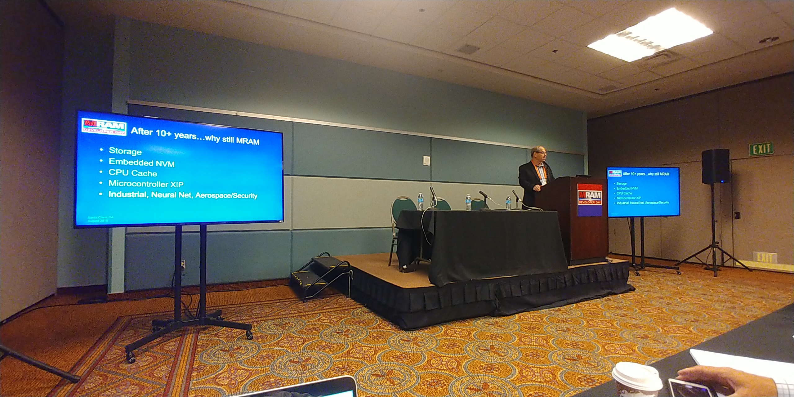
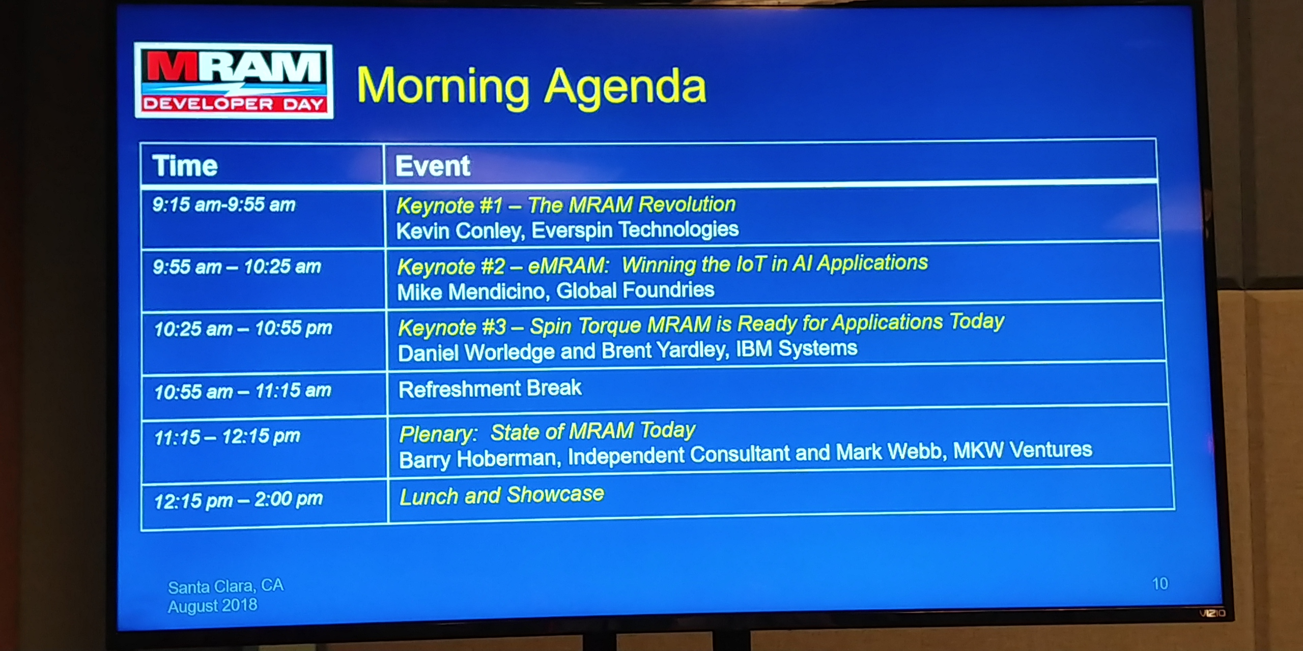
12:01PM EDT - Prior to Flash Memory Summit, the first order of business is the MRAM Developer Day. The key talks today revolve around Everspin, a leader in MRAM Technology, GlobalFoundries, and IBM. First up is Kevin Conley, CTO of Everspin, covering the latest in the 'MRAM Revolution'. The presentation starts at 9:15am PT, and Billy and I are here to cover the event.
12:04PM EDT - Prior to the Everspin presentation, the chair of the session is going through 'Why MRAM'

12:05PM EDT - Some talk about using MRAM in CPU caches in the future later
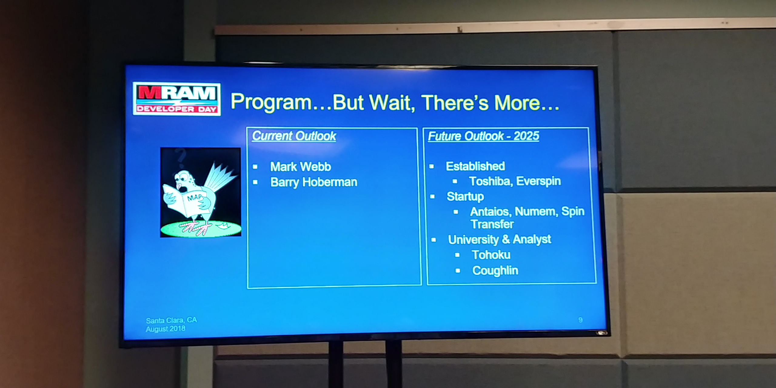
12:06PM EDT - End of the day is a future outlook panel about MRAM in 2025. Unfortunately we'll miss that for another event
12:07PM EDT - Everspin are the only commercial producer of standalone MRAM devices today
12:07PM EDT - Kevin Conley to the stage
12:08PM EDT - Going to talk about the potential to disrupt the industry through MRAM
12:09PM EDT - Driving the future of the industry through innovative products
12:09PM EDT - 'potential futures' defined for legal reasons
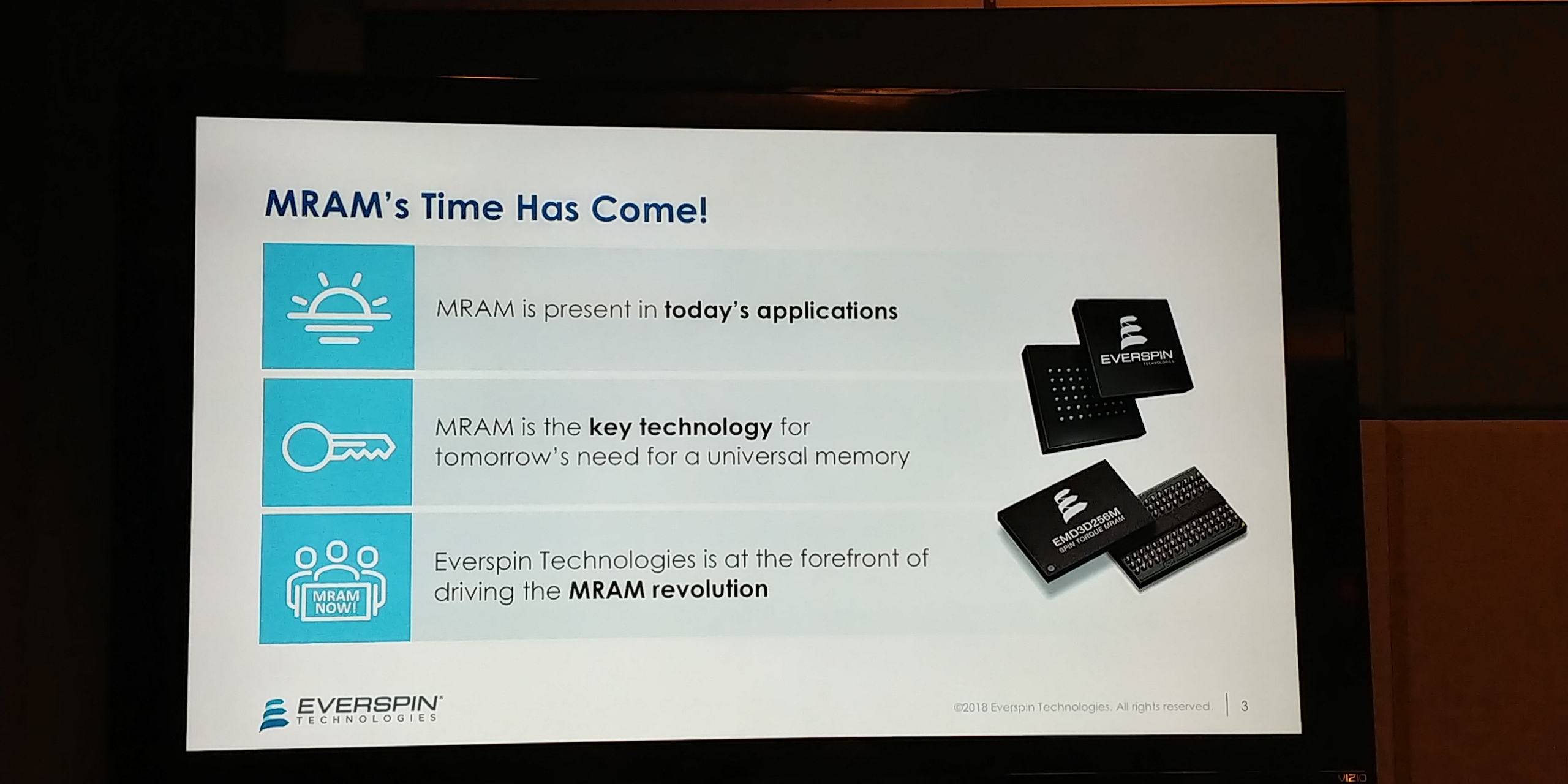
12:09PM EDT - Most discussions on MRAM today is about 'emrging technologies'
12:09PM EDT - But today's discussion is about MRAM uses today
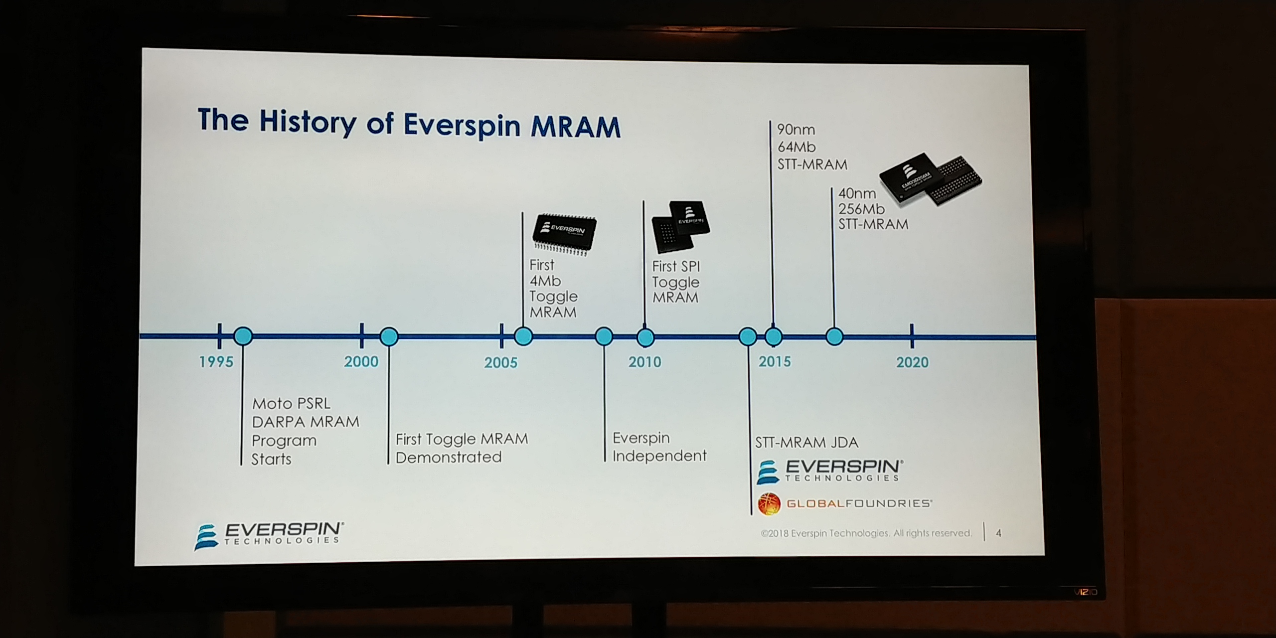
12:10PM EDT - Starting with MRAM History
12:10PM EDT - 1996 MRAM DARPA Program starts
12:10PM EDT - 2001 First Toggle MRAM demonstrated
12:10PM EDT - 2006 First 4 Mb Toggle MRAM
12:11PM EDT - 2008 Everspin spins out of Freescale to become independent
12:11PM EDT - 2010 First SPI Toggle MRAM
12:12PM EDT - 2010 First SPI Toggle MRAM
12:13PM EDT - 2010 First SPI Toggle MRAM
12:13PM EDT - 2014 Spin-Transfer Torque Joint Development Alliance with GloFo
12:14PM EDT - 2015 First demo of STT-MRAM 64Mb chip on 90nm using inhouse
12:14PM EDT - 2018 Mass production of 256 Mb STT-MRAM chip at GloFo
12:14PM EDT - 2018 First 1 Gb chips sampling to customers
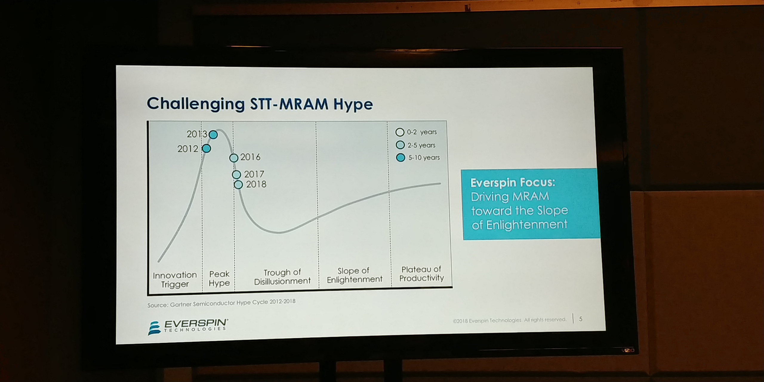
12:14PM EDT - Driving it into the 'slope of enlightment' with multiple suppliers
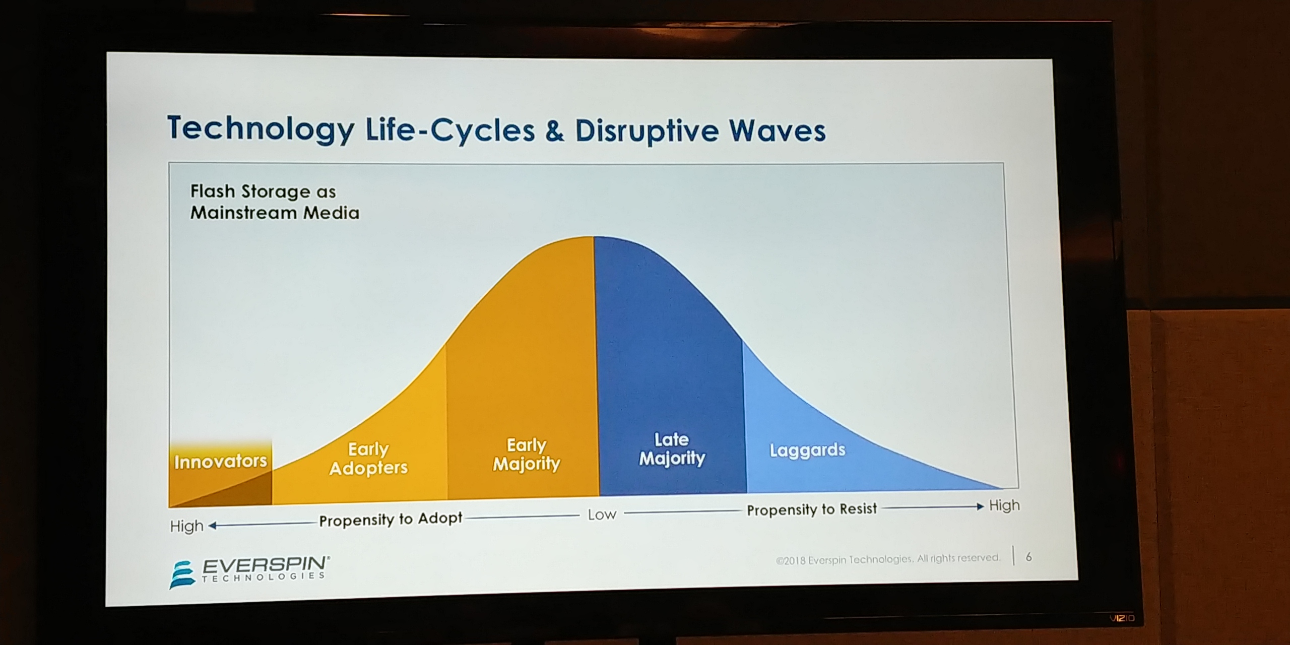
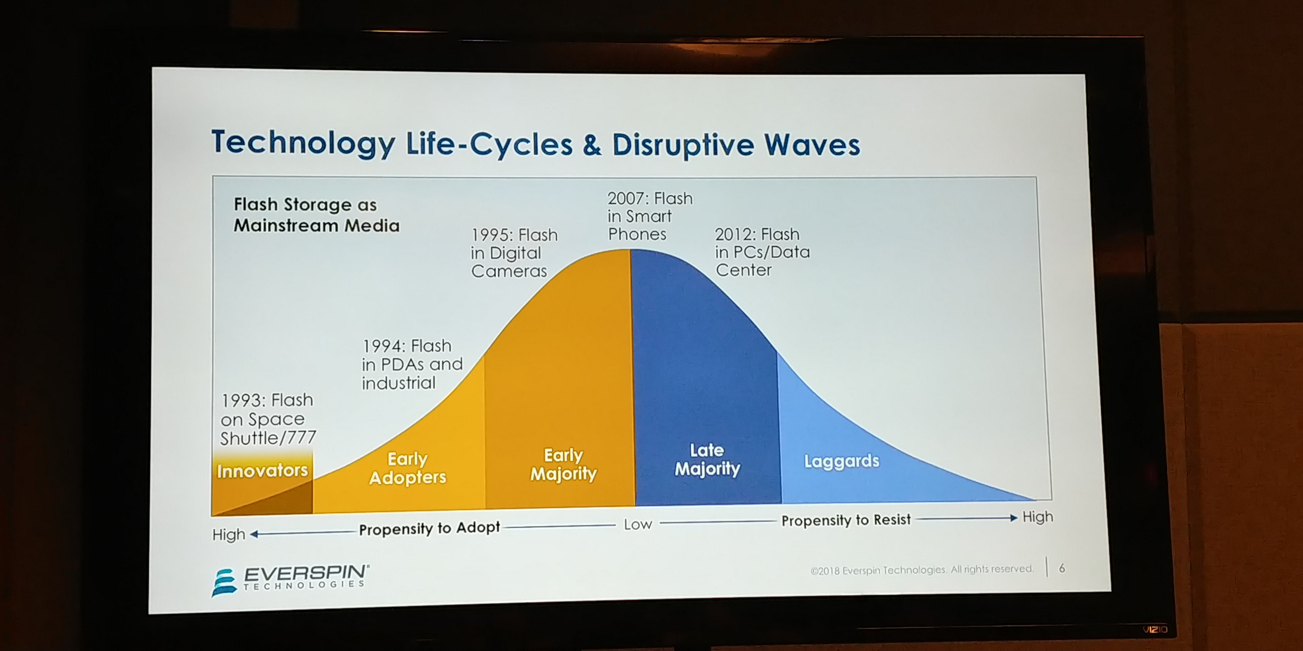
12:16PM EDT - Showing how flash developed from 1993 to today
12:16PM EDT - Flash started as a HDD replacement technology, but went into a variety of markets
12:17PM EDT - The size of flash today is pretty phenomenal
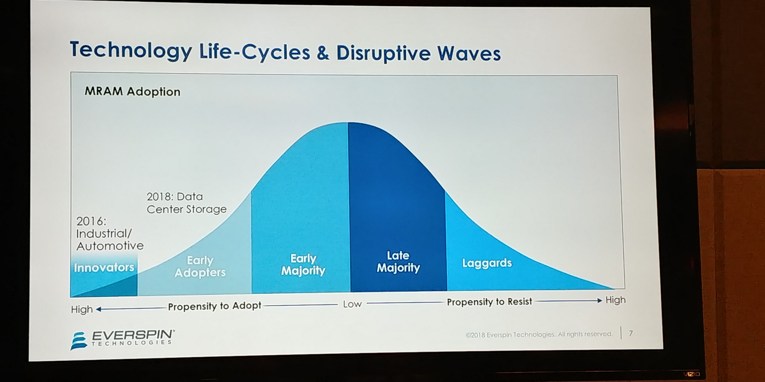
12:17PM EDT - MRAM in 2018 is moving from niche industrial to mainstream storage
12:18PM EDT - All about the early adopters recognizing the usefulness of MRAM
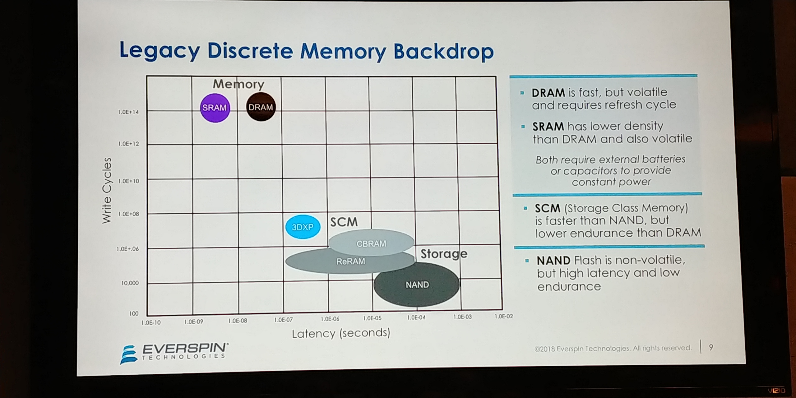
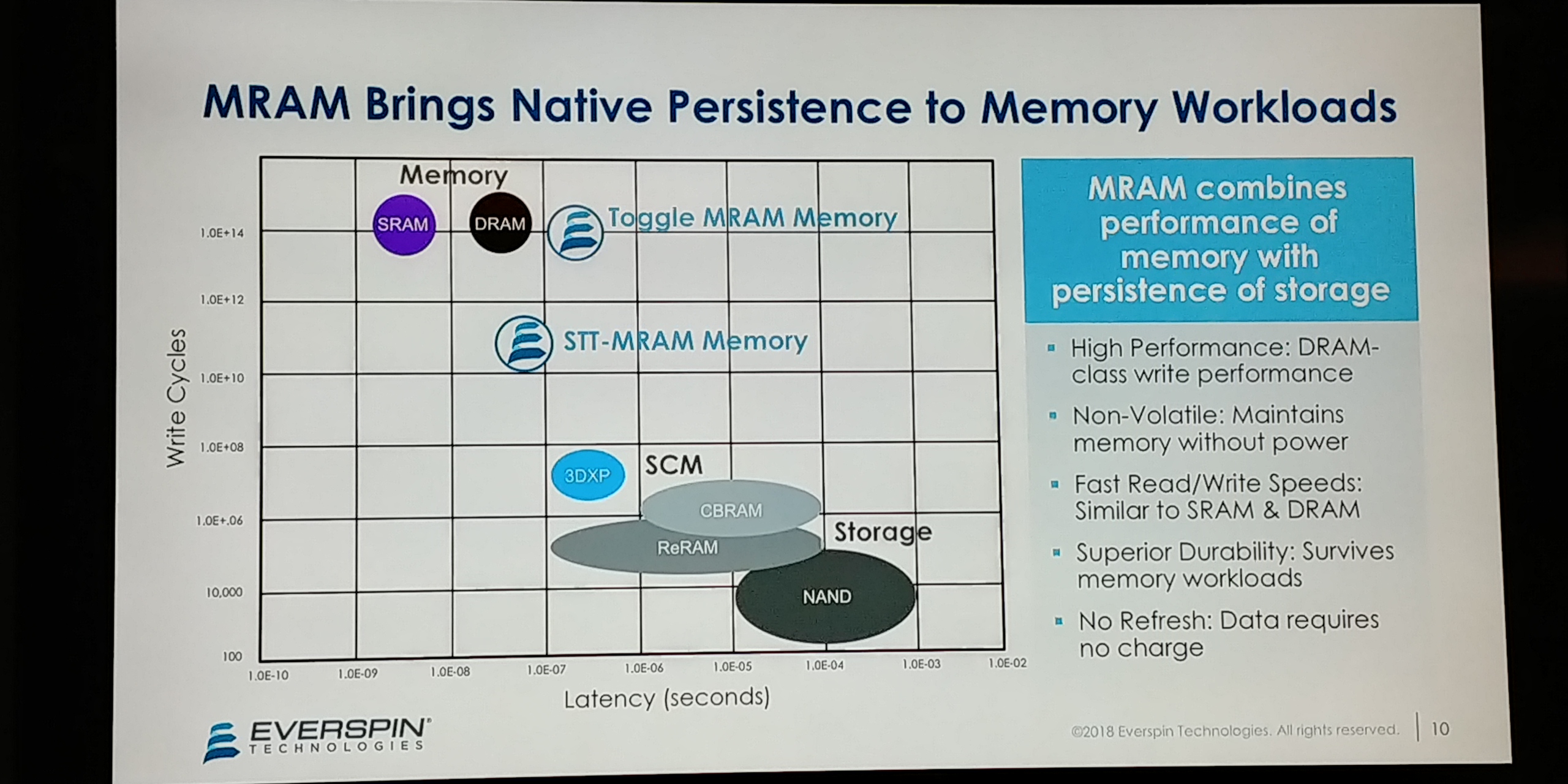
12:18PM EDT - MRAM is viewed from a latency and endurance point of view
12:19PM EDT - MRAM is unique value prop - low latency and high endurance
12:19PM EDT - Separating memories suited for storage (NAND) and those that are carrying memory workloads
12:19PM EDT - The gap between the technologies are quite wide
12:20PM EDT - Even with they hype, storage technologies aren't suited for memory
12:20PM EDT - This is where MRAM comes in
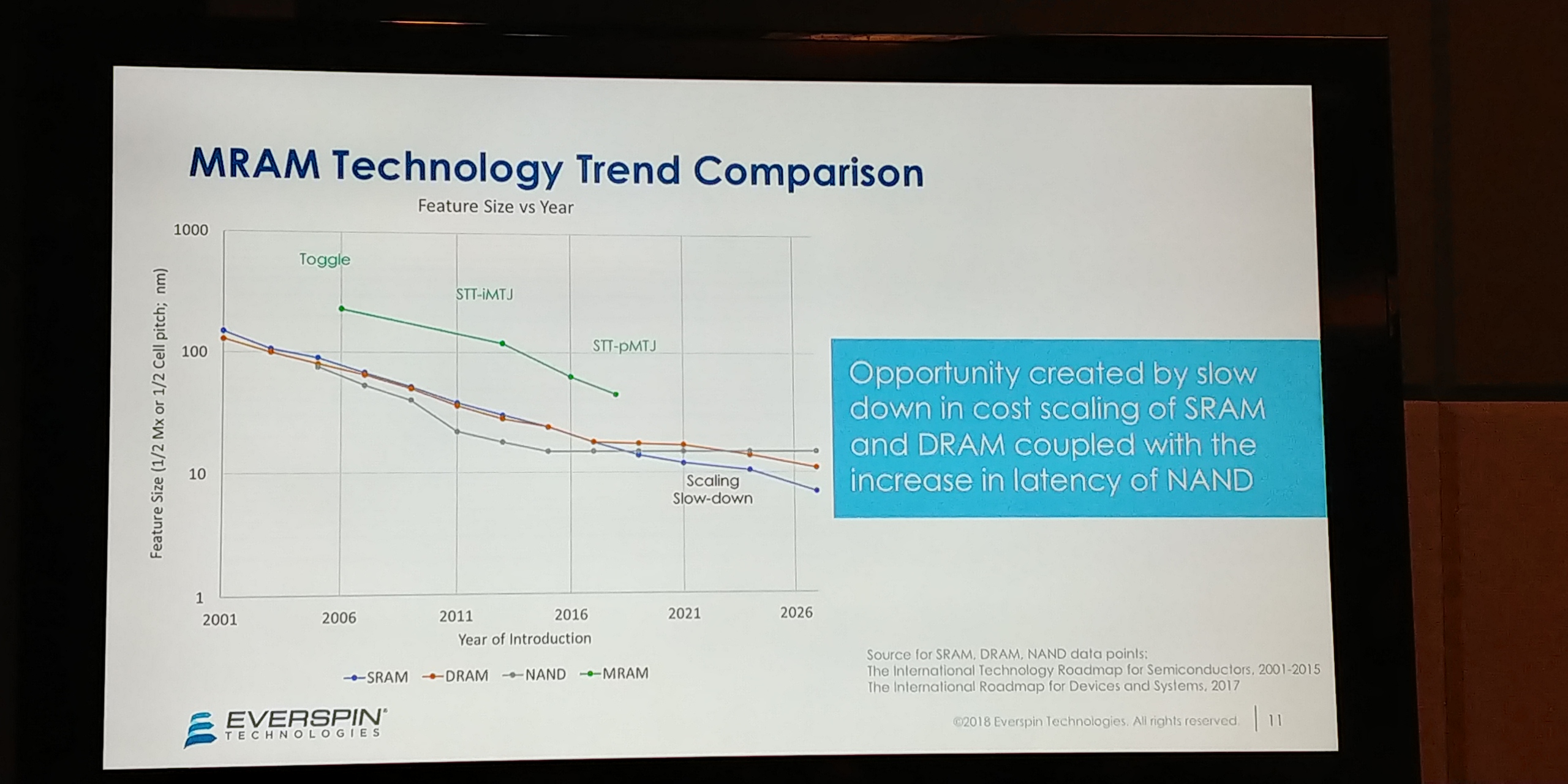
12:20PM EDT - Pace of memory has slowed significantly
12:21PM EDT - DRAM is being challenged by the cost per bit benefits previously experienced, also power and latency
12:21PM EDT - latency is becoming less consistent due to the strength of ECC being used
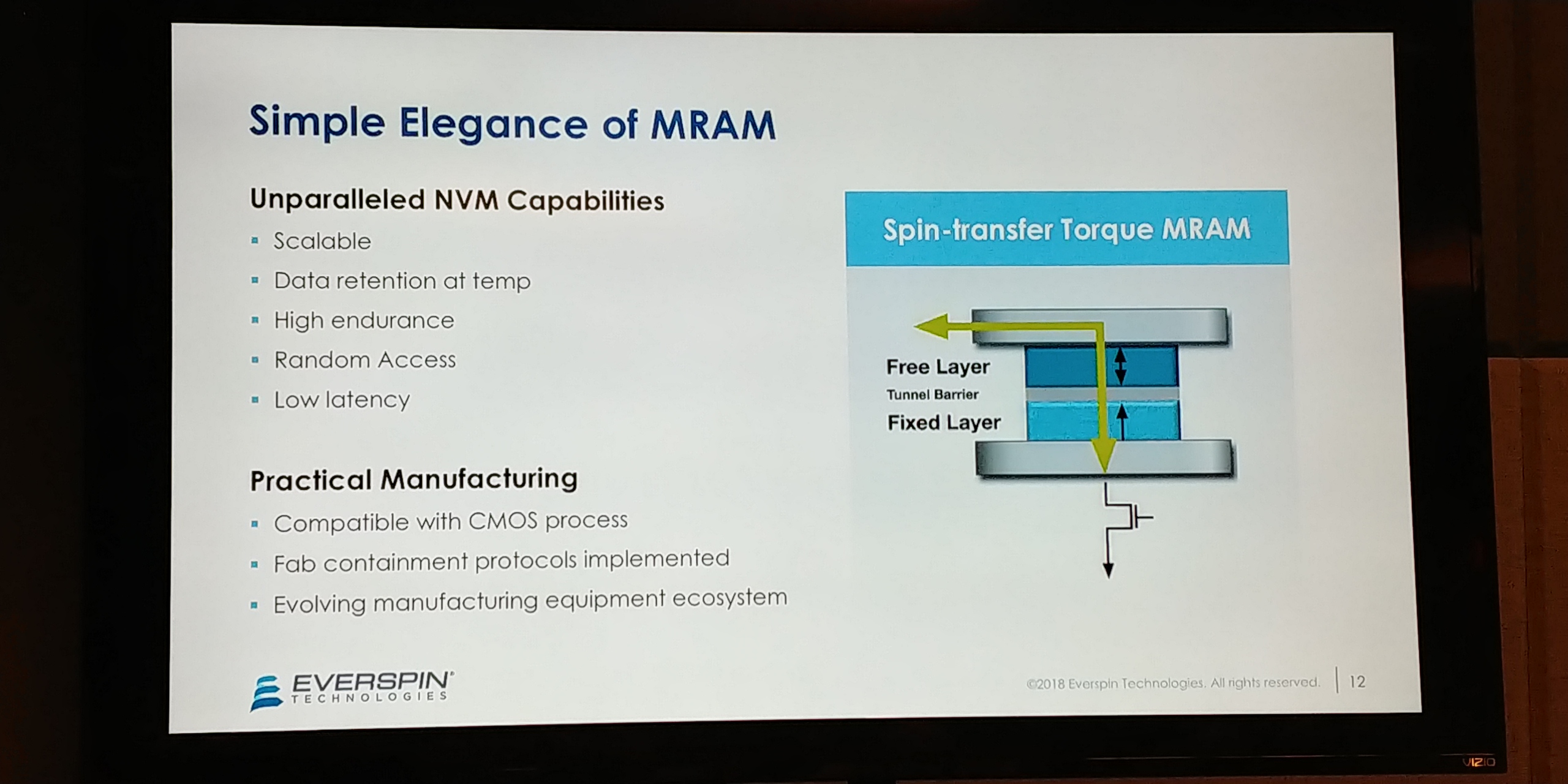
12:21PM EDT - Excitement in how the MRAM technology will scale
12:21PM EDT - Able to retain data at standard temperatures
12:22PM EDT - Able to ensure reflow in industrial processes (260C)
12:22PM EDT - It has become practical to implement MRAM in standard CMOS processes
12:22PM EDT - Fab containment protocols in place and equipment ecosystem is being developed
12:23PM EDT - The MRAM Universe is about the data center - ultra low latency, marhcine learning processor memory, or CPU L2 cache
12:23PM EDT - Most accelerators today are in huge SRAM-based - MRAM focus on scaling is to help here
12:24PM EDT - Also edge applications
12:24PM EDT - MRAM with sensors and compute in infrastructure, security
12:24PM EDT - Tamper resistant and incorruptible memory
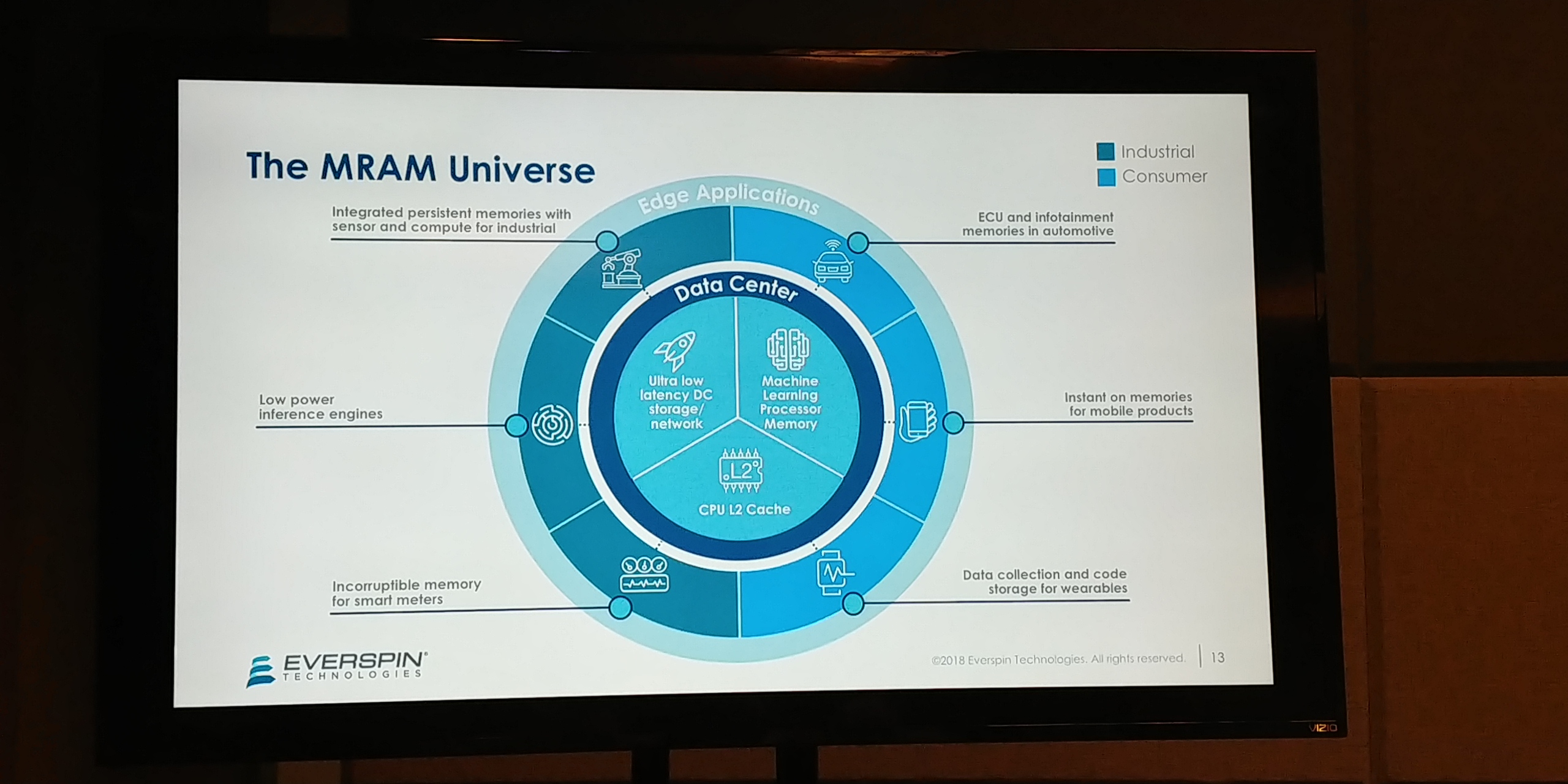
12:25PM EDT - Cars, ADAS, storage for wearables at lower power, instant on memory, etc
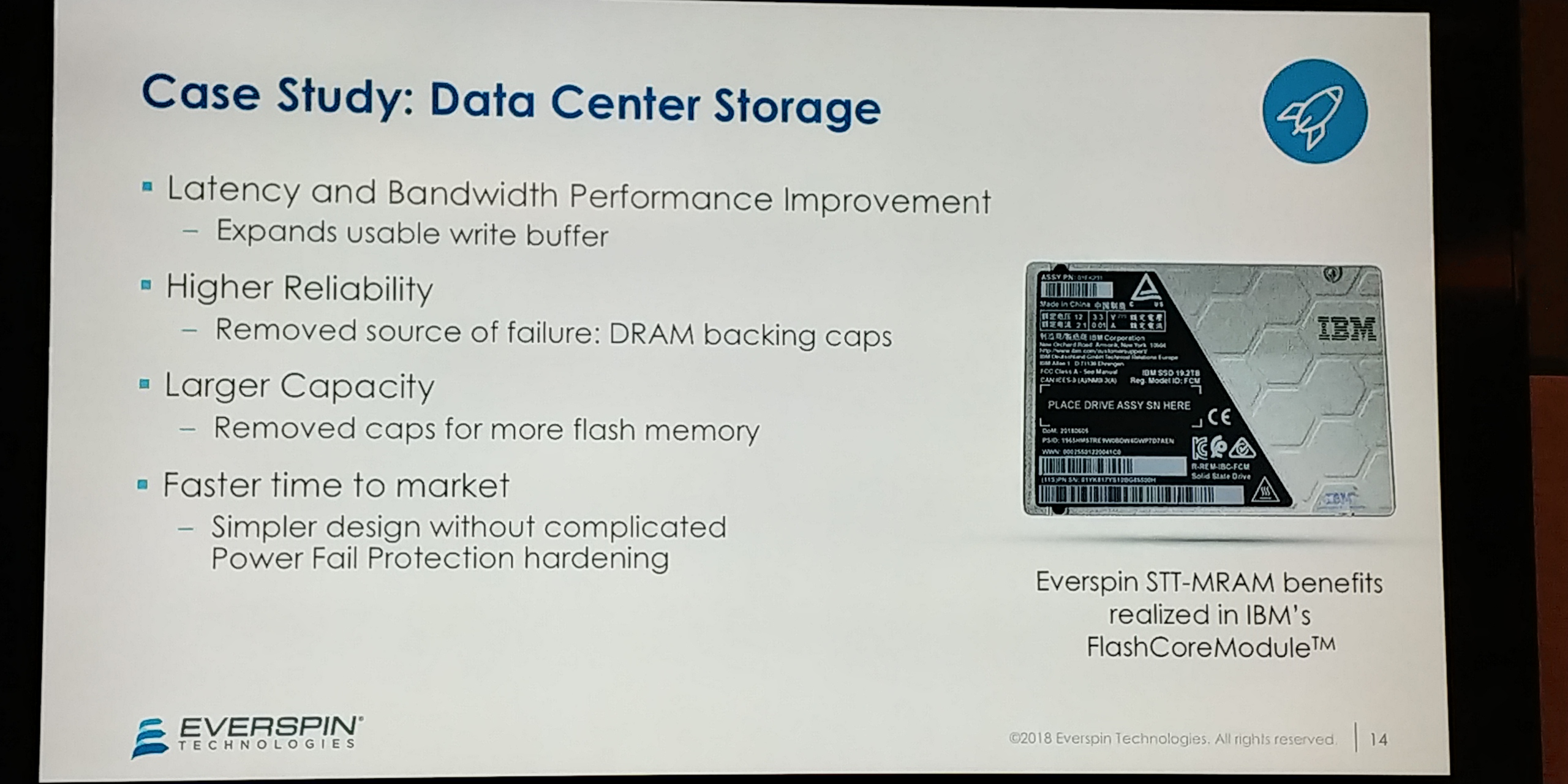
12:26PM EDT - Case study: data center storage. MRAM is used to replace the write buffer
12:26PM EDT - Replacing DRAM with caps due to MRAM
12:27PM EDT - Fewer caps = cost savings plus higher density storage module
12:27PM EDT - Faster time to market without power fail protection hardening - it's baked in
12:28PM EDT - Benefits include QoS due to more data stored in buffers
12:28PM EDT - Bandwidth is limited based on buffers - trade offs are made. These are better with MRAM with larger buffers
12:28PM EDT - Removing caps also improves reliability
12:29PM EDT - Power Fail Protection qualification is usually the last thing on the list - but one of the hardest. By enabling it on the drive automatically speeds up production
12:30PM EDT - IBM will have the first STT-MRAM enabled device on the show floor this week
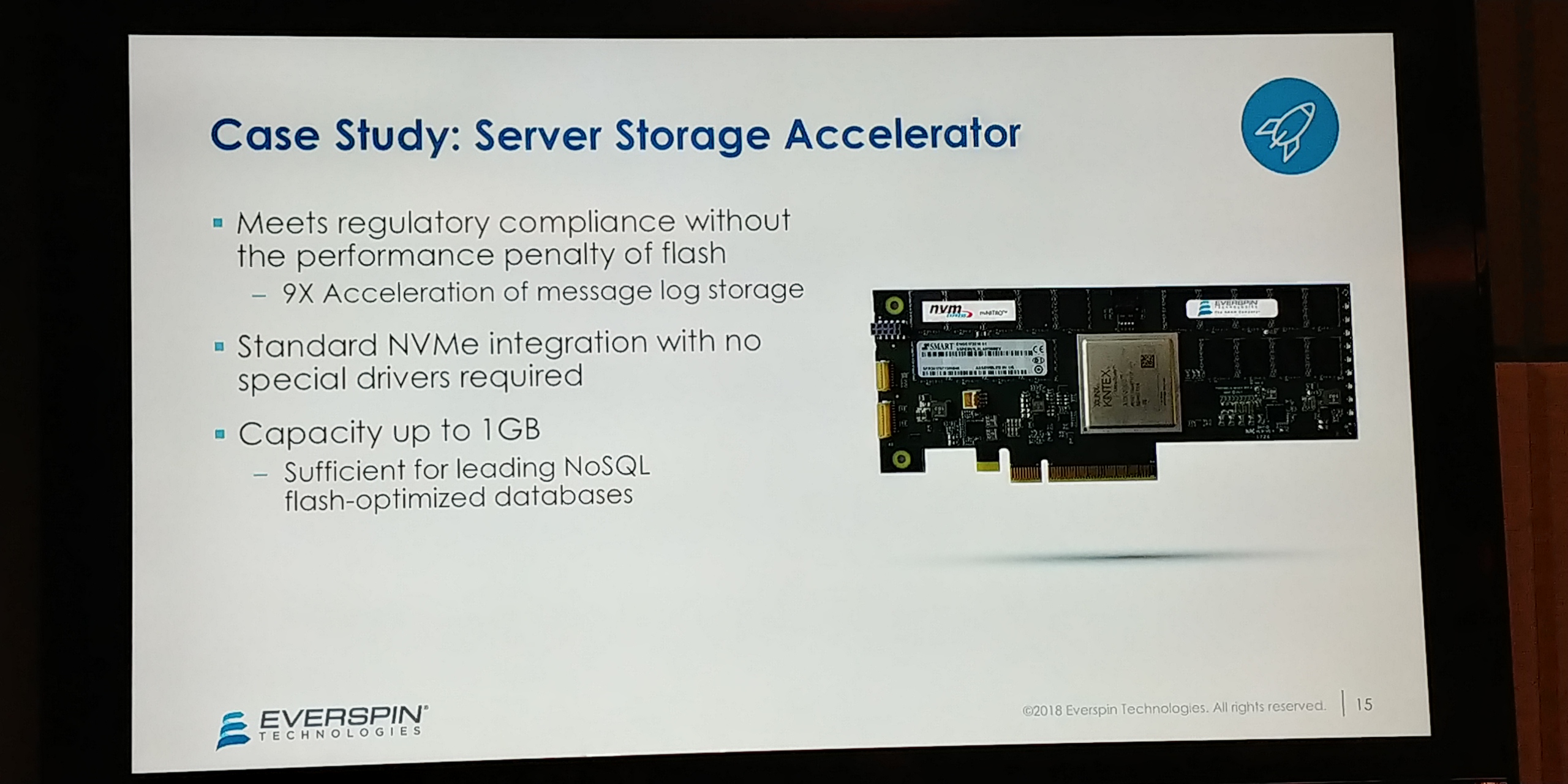
12:30PM EDT - Another Case Study: an All MRAM-storage product
12:31PM EDT - Capacity up to 1GB
12:31PM EDT - Small packets offloaded to lower latency MRAM
12:31PM EDT - 1GB is really good for terabyte-class NoSQL Databases
12:31PM EDT - AI is mostly focused as MRAM replacement in the data center
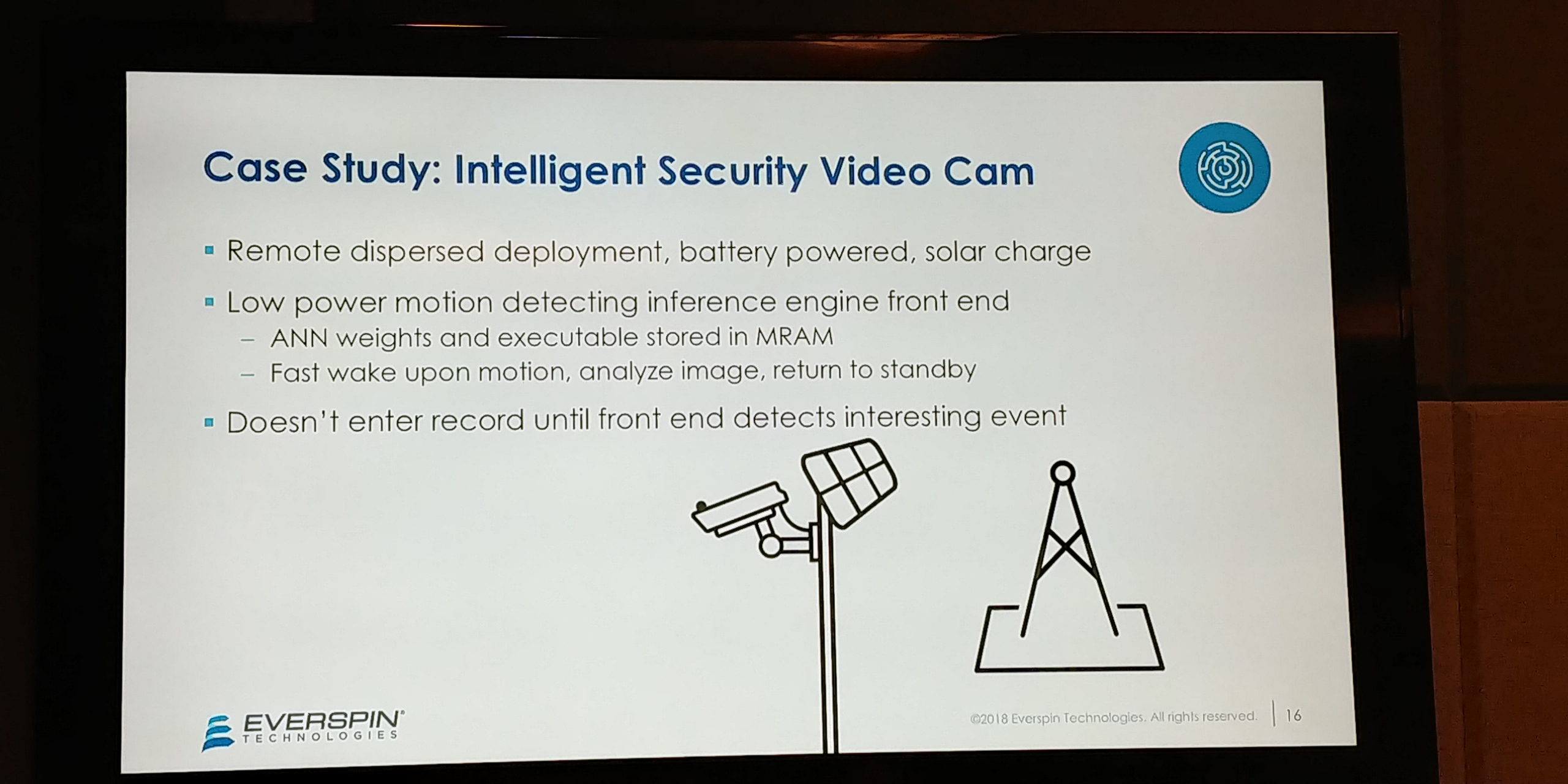
12:32PM EDT - But also applicable at the edge, eg security cameras
12:32PM EDT - Cameras in remote installations that are battery or solar powered
12:32PM EDT - Can be very targeted recording to save power
12:32PM EDT - AI can identify a human vs a cat, and trigger recording appropriately
12:33PM EDT - Traditional AI inference engines should be powered up. NVM allows all the network weights ready to execute
12:33PM EDT - Case Study: Health Wearables
12:35PM EDT - Extended temp operation, longer term integration of AI engines
12:35PM EDT - Next for MRAM - broader adoption in aerospace and industrial
12:35PM EDT - Understanding STT where data persistence at speed is required
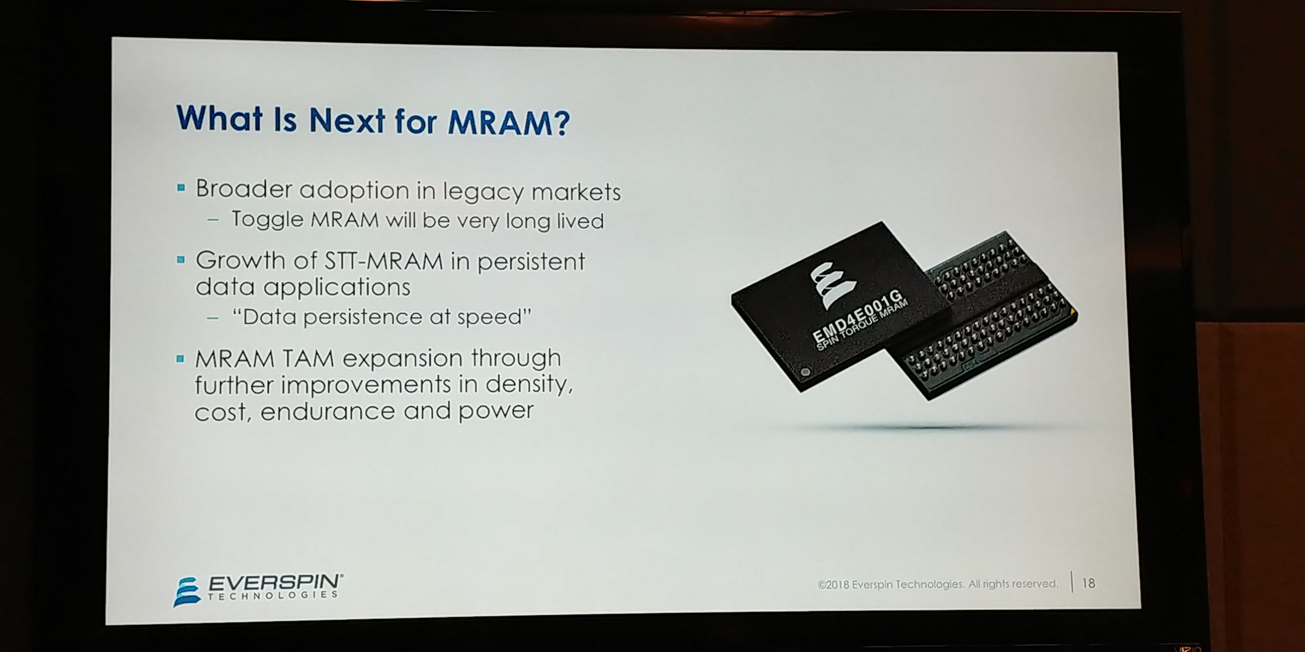
12:36PM EDT - TAM increases as speed, density, increases
12:36PM EDT - Call to action: Define needs in terms of data persistence at speed
12:36PM EDT - Consider transformational impact of MRAM
12:37PM EDT - It's not a problem of cost per bit, it's understanding the product
12:37PM EDT - We have a meeting with Everspin later in the week at FMS
12:37PM EDT - That's a wrap!


3 Comments
View All Comments
vortmax2 - Monday, August 6, 2018 - link
Very interesting. Samples already...let's see where this goes!Santoval - Monday, August 6, 2018 - link
I've read that switching speeds of 750 ps (that's picosecond, i.e. 0.75 ns!) have been achieved by researchers, though presumably by employing a 3 terminals and 2 transistors per cell, thus sacrificing half the density. Assuming a comparable process node with SRAM so that the features are roughly the same size, that is still 3 times the density of SRAM.Even if it is impractical or makes no sense to use 3-terminal STT-MRAM for L1 cache, it could still be used for ultra fast L2 cache, while employing a standard (but faster than the current MRAM) 2-terminal - 1 transistor MRAM for L3 cache. I cannot easily assess the potential latency gain, but even if there was none due to the progressively increased size, CPUs could have 3 times the L2 cache and 6 times the L3 cache at the same size as having 1/3 the L2 and 1/6 the L3 SRAM cache!
boozed - Wednesday, August 8, 2018 - link
The "MRAM revolution", like flying cars and cold fusion and hoverboards?