Western Digital: Nearly All NAND Capacities Resumed Normal Operations
by Anton Shilov on August 1, 2019 4:00 PM EST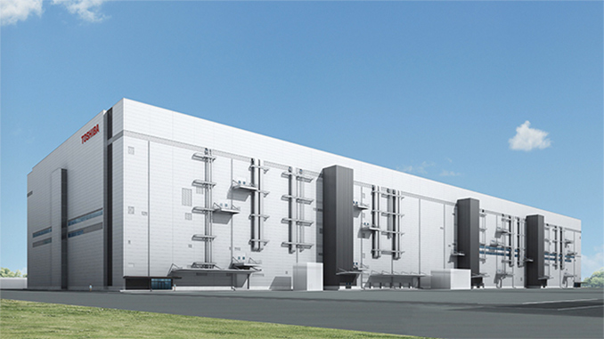
Western Digital and its manufacturing partner Toshiba Memory Co. (TMC) had managed to resume normal operation of almost all of their joint production lines at their Yokkaichi Operations campus in Japan, Western Digital said on Wednesday. Damages to wafer and manufacturing tools will cost Western Digital up to $339 million in total.
A 13-minute unexpected power outage in the Yokkaichi province in Japan on June 15 affected the manufacturing facilities jointly operated by Western Digital and TMC. The incident damaged wafers that were processed and also production equipment used by the companies. Western Digital said in late June that the accident would reduce its NAND flash wafer supply in Q3 by approximately 6 EB (exabytes), which was believed to be about a half of the company’s quarterly supply of NAND. Toshiba also confirmed that wafers and equipment was damaged, but did not elaborate.
By now, virtually all production capacities at the Yokkaichi Operations are back online, according to Steve Milligan, chief executive of Western Digital.
“Western Digital and TMC teams have worked diligently on recovery activities and as of now, nearly all of the equipment in the fabs has returned to normal operations.”
The company believes that all the lost wafers will be contained in the September quarter, but the incurred damages will be quite vast. In Q4 FY2019 (Q2 C2019) the company took a $145 million charge for impacted equipment as well as operations, and plans to take another $170 – $190 million write-off in the September quarter. As a result, the impact on Western Digital will total $315 – $339 million.
Being a private company, Toshiba Memory does not disclose the impact of the accident, but if the company lost the equal number of wafers and has had to restore its production capacities, so its losses will be comparable to those of Western Digital. Overall, the 13-minute power outage will cost the two companies $630 to $678 million.
Related Reading:
- Toshiba & WD NAND Production Hit By Power Outage: 6 Exabytes Lost
- Toshiba Memory and Western Digital Open Fab 6 and New Memory R&D Center
- Toshiba Memory & Western Digital Finalize Fab K1 Investment Agreement
- Toshiba Begins to Construct New BiCS 3D NAND Fab in Iwate Prefecture
- Toshiba Memory to Build New Fab to Produce BiCS 3D NAND
- Toshiba Finalizes Plans for New 3D NAND Fab: Coming Online in 2019
- Toshiba to Build New Fab to Produce BiCS NAND Flash
Source: Western Digital


30 Comments
View All Comments
yacoub35 - Thursday, August 1, 2019 - link
Would love to know how/why a power outage could cause so much damage. And who was responsible for risk assessment and mitigation at the plant that didn't build the functions to survive a power outage without that sort of outcome.euskalzabe - Friday, August 2, 2019 - link
Exactly my thoughts. You can smell the price fixing from miles away. Disgusting.edzieba - Friday, August 2, 2019 - link
No need to manufacture power outages or stage floods. Fab companies who want to drop production due to oversupply take the much simpler route of making a public announcement (usually as part of an investor call or other financial filing) that they are dropping output due to oversupply.Yojimbo - Friday, August 2, 2019 - link
That's not price fixing... Reducing production is not price fixing or collusion..Yojimbo - Friday, August 2, 2019 - link
Price fixing? Do you think the accident didn't happen? The wafers weren't really destroyed? Or you think WD and Toshiba just "took one for the team"? I suppose Airbus and Boeing are similarly price fixing for aircraft by crashing two of Boeing's aircraft.Sahrin - Friday, August 2, 2019 - link
Yeah, they kind of are. They are both paying huge bribes to right wing politicians to deregulate them, which is the ultimate cause of the accident.Manch - Tuesday, August 6, 2019 - link
So it's Trumps fault?! LOLDanNeely - Friday, August 2, 2019 - link
There was backup power, the outage lasted longer than the backup lasted.The reason the losses were so extensive is that you can't stop any wafer step midway through without ruining it; and it takes a few months to go from a blank wafer of silicon to one that's ready to be cut into individual dies; so when the outage exceeded the onsite backup runtime it killed every wafer that was in progress inside a machine at the time; which was roughly half the quarterly output of the plant.
buxe2quec - Friday, August 2, 2019 - link
I was also getting to the conclusion that a wafer must takes weeks for the processing, but I'm still amazed that that's the case. Weeks/months from the first photolithography to the ready die? that way more than I thought. At 96 layers, that's one day per layer!Kristian Vättö - Friday, August 2, 2019 - link
It takes ~3 months to produce a 3D NAND wafer and there are over 400 steps in the process.