Arm Announces Ethos-N78 NPU: Bigger And More Efficient
by Andrei Frumusanu on May 27, 2020 10:00 AM EST
Yesterday Arm released the new Cortex-A78, Cortex-X1 CPUs and the new Mali-G78 GPU. Alongside the new “key” IPs from the company, we also saw the reveal of the newest Ethos-N78 NPU, announcing Arm’s new second-generation design.
Over the last few years we’ve seen a literal explosion of machine learning accelerators in the industry, with a literal wild west of different IP solutions out there. On the mobile front particularly there’s been a huge amount of different custom solutions developed in-house by SoC vendors, this includes designs such as from Qualcomm, HiSilicon, MediaTek and Samsung LSI. For vendors who do not have the design ability to deploy their own IP, there’s the possibility of licensing something from an IP vendor such as Arm.
Arm’s “Ethos” machine learning IP is aimed at client-side inferencing workloads, originally described as “Project Trillium” and the first implementation seeing life in the form of the Ethos-N77. It’s been a year since the release of the first generation, and Arm has been working hard on the next iteration of the architecture. Today, we’re covering the “Scylla” architecture that’s being used in the new Ethos-N78.
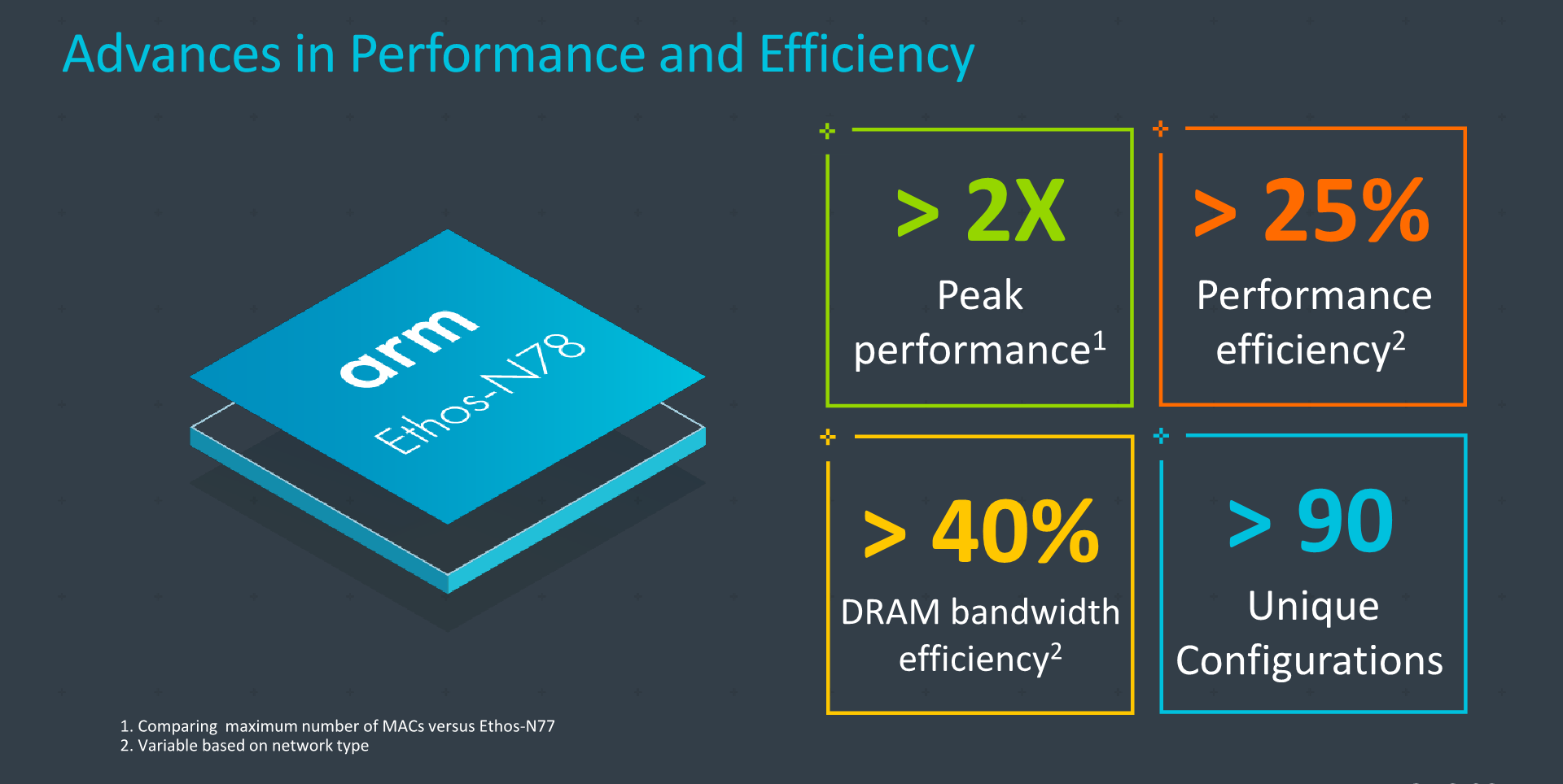
From a very high-level view, what the N78 promises is a quite large boost both in performance and efficiency. The new design scales up much higher than the biggest N77 configuration, now being able to offer 2x the peak performance at up to 10TOPs of raw computational throughput.
Arm has revamped the design of the NPU for better power efficiency, enabled through various new compression techniques as well as an improvement in external memory bandwidth per inference of up to 40%.

Strong points of the N78 are the IP’s ability to scale performance across different configuration options. The IP is available at 4 different performance points, or better said at four different distinct engine configurations, from the smallest config at 1TOPs, to 2, 5 and finally a maximum of 10TOPs. This corresponds to MAC configurations of 512, 1024, 2048 and 4096 units for the totality of the design.
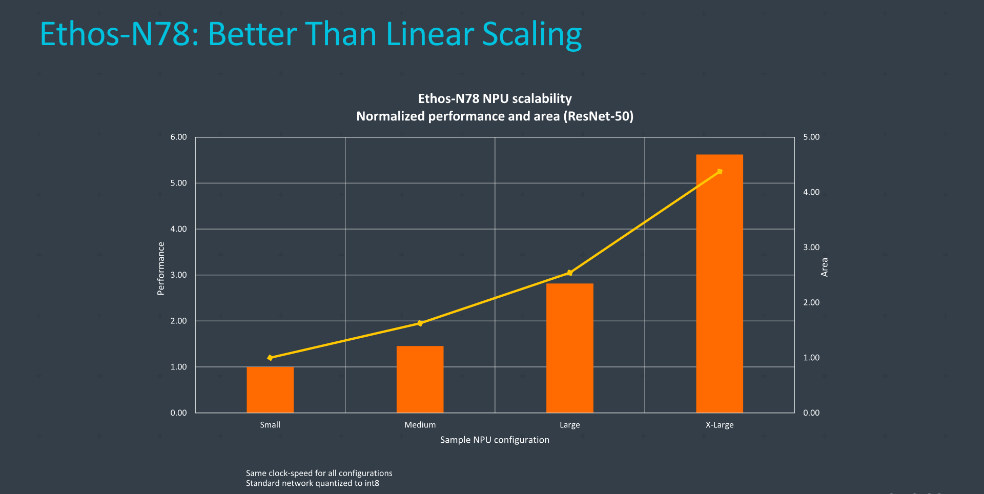
The interesting aspect of scaling bigger is that the area efficiency of the IP actually scales better the bigger the implementation, due to probably the fact that the unique fixed shared function blocks area percentage shrinks with the more computation engines the design has.
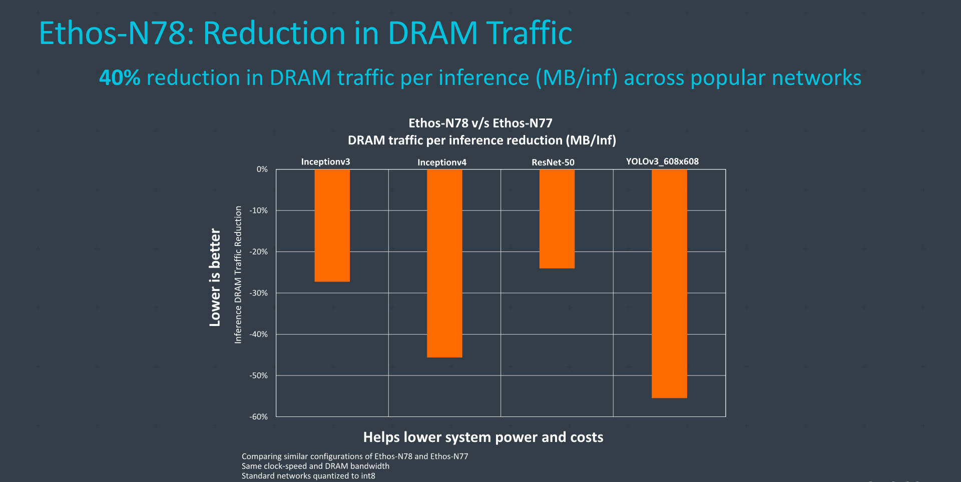
Architecturally, the biggest improvements of the new N78 were in the way it handles data around in the engines, enabling new compression methods for data that not only goes outside the NPU (DRAM bandwidth improvement), but also data movement within the NPU itself, improving efficiency for both performance and power.
The new compression and data handling can significantly reduce the bandwidth of the system with an average 40% reduction across workloads – which is an extremely impressive figure to showcase between IP generations.
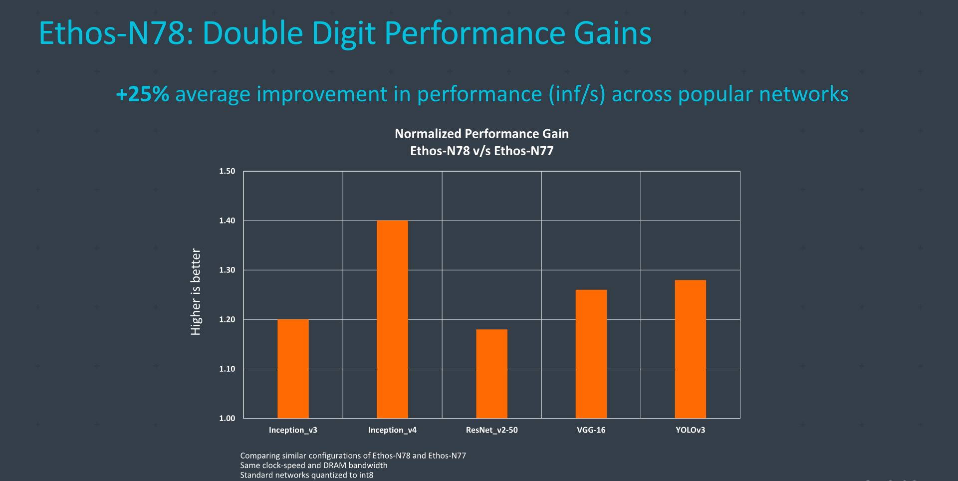
Generational performance uplifts, thanks to the higher performance density and power efficiency are on average 25%, which along with the doubled peak performance configuration means that it has the potential to represent a large boost in end devices.
It’s quite hard to analyse NPUs on how they perform in the competitive landscape – particularly here in Arm’s case given that we haven’t yet seen the first generation NPU designs in silicon. One interesting remark that Arm has made, is that in this space, software matters more than anything else, and a bad software stack can possibly ruin what otherwise would be a good hardware design. Arm mentioned they’ve seen vendors adopt their own Ethos IP and dropping competitor designs because of this – Arm says they invest a very large amount of resources into software in order to facilitate customers to actually properly make use of their hardware designs.
Arm’s new Ethos-N78 has already been licensed out to customers and they’re taping in their designs with it, with likely the first products seeing the light of day in 2021 at the earliest.
Related Reading:
- Arm Announces New Ethos-N57 and N37 NPUs, Mali-G57 Valhall GPU and Mali-D37 DPU
- ARM Details "Project Trillium" Machine Learning Processor Architecture
- Imagination Goes Further Down the AI Rabbit Hole, Unveils PowerVR Series3NX Neural Network Accelerator
- CEVA Announces NeuPro-S Second-Generation NN IP
- Cadence Announces Tensilica Vision Q7 DS


34 Comments
View All Comments
Operandi - Wednesday, May 27, 2020 - link
Ok.....whats an NPU?psychobriggsy - Wednesday, May 27, 2020 - link
Neural Processing UnitAI accelerator
PeachNCream - Wednesday, May 27, 2020 - link
A marketing buzzword. It's like saying your company "leverages cloud computing" instead of saying, "We're buying computer resources from a third party."kaidenshi - Wednesday, May 27, 2020 - link
Except in this case, it's accurate. NPUs are designed for AI work, just as GPUs are designed for graphics processing. I get clutching pearls over "the cloud" and the terrible buzzword-heavy language surrounding it, but this ain't that.rahvin - Wednesday, May 27, 2020 - link
I get the buzzword weariness you comment on but no one can honestly deny the impact cloud computing has had, both on the industry at large and all the businesses it touches. Cloud computing has completely altered the industry.And the GP should consider the impact NPU's have had and just how many of them are being produced. NPU's have significantly different workloads than both CPU's and GPU's. The workloads can be shoehorned onto both the prior chips but at a high cost in efficiency. The NPU's that first showed up with Google's Tensor processor more than 10 years ago have been growing exponentially in deployments. If you are curious about there is plenty of information out there on why google developed the Tensor NPU and why they continue to develop and refine it. [In particular I remember an article discussing when google first deployed Google assistant and realized that if even 3% of android users used the assistant at once it would overwhelm all of Google's compute resources.[
Almost every major CPU producer now has a separate NPU unit in production and the number being sold is growing at nearly exponential rates. For example, every Pixel phone since the second generation has included a separate google designed NPU and most of the other phone producers have followed suit with NPU's of their own in the most recent generations after seeing the benefits this chip provided to the pixel phones.
NPU's are here to stay and will be growing and developing likely as fast as GPU's did. Though they won't have the retail deployment like GPU's did you're likely to see them deployed, if not directly into products into the back-end that serves them, even if you don't know they are there.
Zoolook - Wednesday, May 27, 2020 - link
Math coprocessors is nothing new, I prefer TPU for Tensor processor unit, NPU is a "buzzword", it's just a very specialized math processor for tensors, much as an FPU for floating point. There is nothing neural about them at all.p1esk - Wednesday, May 27, 2020 - link
There's nothing "tensor" about these math coprocessors. They are designed to multiply regular 2D matrices. Lots of multiply accumulate ops performed in parallel on two wide input vectors. Typically the inputs are FP16 (e.g. Google TPU), or INT8 (this one).sun_burn - Wednesday, May 27, 2020 - link
That depends on the design of the accelerator. Some accelerators are systolic array matrix multipliers . Others implement dot product multipliers that operate on the native tensor without conversion to 2D matrix form .p1esk - Wednesday, May 27, 2020 - link
Which ones operate on native tensor without conversion to 2D matrix form?sun_burn - Wednesday, May 27, 2020 - link
That’s not something that it appears companies reveal when it comes to NPUs. The information just gets encapsulated in the blob ‘N MACs’ . For example 4096 MACs could be a 64x64 matrix multiplier, or a 16x16x16 dot product multiplier stack. It may be possible to infer it indirectly.