SiPearl Lets Rhea Design Leak: 72x Zeus Cores, 4x HBM2E, 4-6 DDR5
by Andrei Frumusanu on September 8, 2020 9:00 AM EST
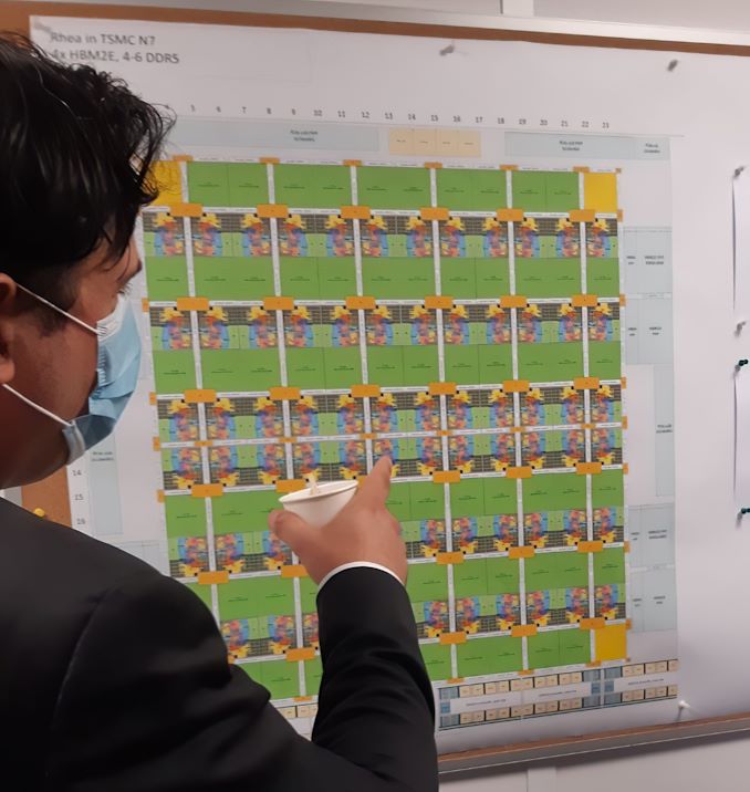
In what seems to be a major blunder by the SiPearl PR team, a recent visit by a local French politician resulted in the public Twitter posting in what looks like the floor plan of the company’s first-generation server chip project “Rhea”.
During a visit of Alexandra Dublanche, a local Île-de-France politician and vice president of economic development and other responsibilities for the region, the PR teams had made some photo-op captures of a tour of the office. Amongst the published pictures includes a shot of the company’s Rhea server chip project with some new, until now unreleased details of the European Processor Initiative-backed project.
Accélérer le développement européen de microprocesseurs à haute performance est un enjeu de souveraineté 🇪🇺
— Alexandra Dublanche (@ADublanche) September 8, 2020
C’est le défi auquel s’attaque la pépite technologique @SIPEARL_SAS basée à #MaisonsLaffitte en @iledefrance
La Région sera à ses côtés face à cet enjeu majeur! pic.twitter.com/kcBwghlfsP
In a close-up and up-scaling of the image, we can see that it’s a detailed floor-plan of the server SoC Rhea, labelled for a target TSMC 7nm process.
We can detail 72 CPU cores and 68 mesh network L3 cache slices in the floor plan, surrounded by various IP whose labels are too small to be legible. SiPearl had previously confirmed that the project uses Arm’s upcoming Neoverse “Zeus” cores which succeed the Neoverse N1 Ares cores that are being used in current generation Arm server SoC designs such as Amazon’s Graviton2 or Ampere’s Altra.
Beyond the confirmation of a core-count, we also see that the Rhea design sports a high-end memory subsystem, with the floor plan labelled as having 4x HBM2E controllers and 4-6 DDR5 controllers. Such a hybrid memory system would allow for extremely high bandwidth to be able to feed such a large number of cores, while still falling back to regular DIMMs to be able to scale in memory capacity.
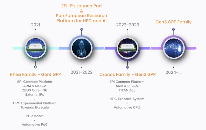
The Rhea family of processors is roadmapped to come to market in 2021. The only curious divergence here is that SiPearl previously stated that this was an N6 project, whilst the recent Twitter picture states it being N7. Given that both processes are design compatible, it might just be a recent shift in the project, or the company still plans to productise it in the N6 node when it comes to market.
The design’s aggressive memory subsystem with the inclusion of HBM2E points out that the company is aiming for quite high performance targets, joining the ranks of Fujitsu in terms of designing a CPU with advanced HBM memory.
Related Reading:
- European Processor Initiative Backed SiPearl Announces Licensing of Arm Zeus Neoverse CPU IP
- Amazon's Arm-based Graviton2 Against AMD and Intel: Comparing Cloud Compute
- Next Generation Arm Server: Ampere’s Altra 80-core N1 SoC for Hyperscalers against Rome and Xeon
- Ampere’s Product List: 80 Cores, up to 3.3 GHz at 250 W; 128 Core in Q4
- A Success on Arm for HPC: We Found a Fujitsu A64FX Wafer
- New #1 Supercomputer: Fugaku in Japan, with A64FX, take Arm to the Top with 415 PetaFLOPs


27 Comments
View All Comments
webdoctors - Tuesday, September 8, 2020 - link
Weird, I thought HBM latency not as good as regular DRAM. Also the memory capacity is tiny right? Like you see cards with only 16GB HBM but servers can have 256 or more GBs of regular DRAM.surt - Tuesday, September 8, 2020 - link
HBM generally has better latency and bandwidth characteristics than DRAM. In some scenarios nearly twice better. The trade-off you correctly note is capacity.edzieba - Tuesday, September 8, 2020 - link
HBM has improved bandwidth, but access latency suffers (up to 20% compared to DDR: https://arxiv.org/pdf/1704.08273.pdf), similar to GDDR vs. DDR. As your interface becomes more parallel, latency to retrieve any given bit goes up (wider & lower clocked vs. narrower and higher clocked bus).anonomouse - Tuesday, September 8, 2020 - link
The “HBM” in that paper is based on Hybrid Memory Cube, not the Jedec HBM. HMC has a very different interface and access model from HBM2, so it’s not clear that the latency conclusions from that apply at all. In particular, HMC has a high speed serdes component for the actual link between memory stacks and the main processor, whereas HBM2 keep the interface wide (which necessitates the silicon interposed).brucethemoose - Tuesday, September 8, 2020 - link
HBM2E supports up to 24GB a stack, but IDK if anyone is shipping more than 16GB.psychobriggsy - Tuesday, September 8, 2020 - link
4 HBM2e could handle up to 96GB I believe, with 24GB stacks (12Hi) - although more likely it will be a 32GB and 64GB configuration. HBM shouldn't have higher latency than off-package DRAM surely!It could be the system uses the HBM as a massive L4 cache, or memory is partitioned under software control so you can put the data where you like, and so on.
CajunArson - Tuesday, September 8, 2020 - link
72 cores? HBM and DDR?I remember when the usual suspects called that a dumb idea 5 years ago when Intel actually put it on the market. Of course, they don't make chips.
Looks like the people who do make chips were busy taking notes and copying the idea.
TeXWiller - Tuesday, September 8, 2020 - link
Just think of all the crazy glue required between the memory chips for pinning, blocking, streaming and the general scratchpaddery! ;)edzieba - Tuesday, September 8, 2020 - link
Larrabee / Xeon Phi (same die, different names) really was ahead of its time. Whatever happened to HMC, anyway?SarahKerrigan - Tuesday, September 8, 2020 - link
HMC is dead. IBM's OMI sometimes feels like a bit of a spiritual sequel to it ("move memory controller to the endpoint and fan out from it; connect to the CPU with fast serial links") but doesn't do the stacking part.