GlobalFoundries To Build New 450K Wafer-per-Year Fab in Singapore
by Ryan Smith on June 22, 2021 3:00 AM EST- Posted in
- Semiconductors
- GlobalFoundries
- 40nm
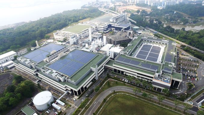
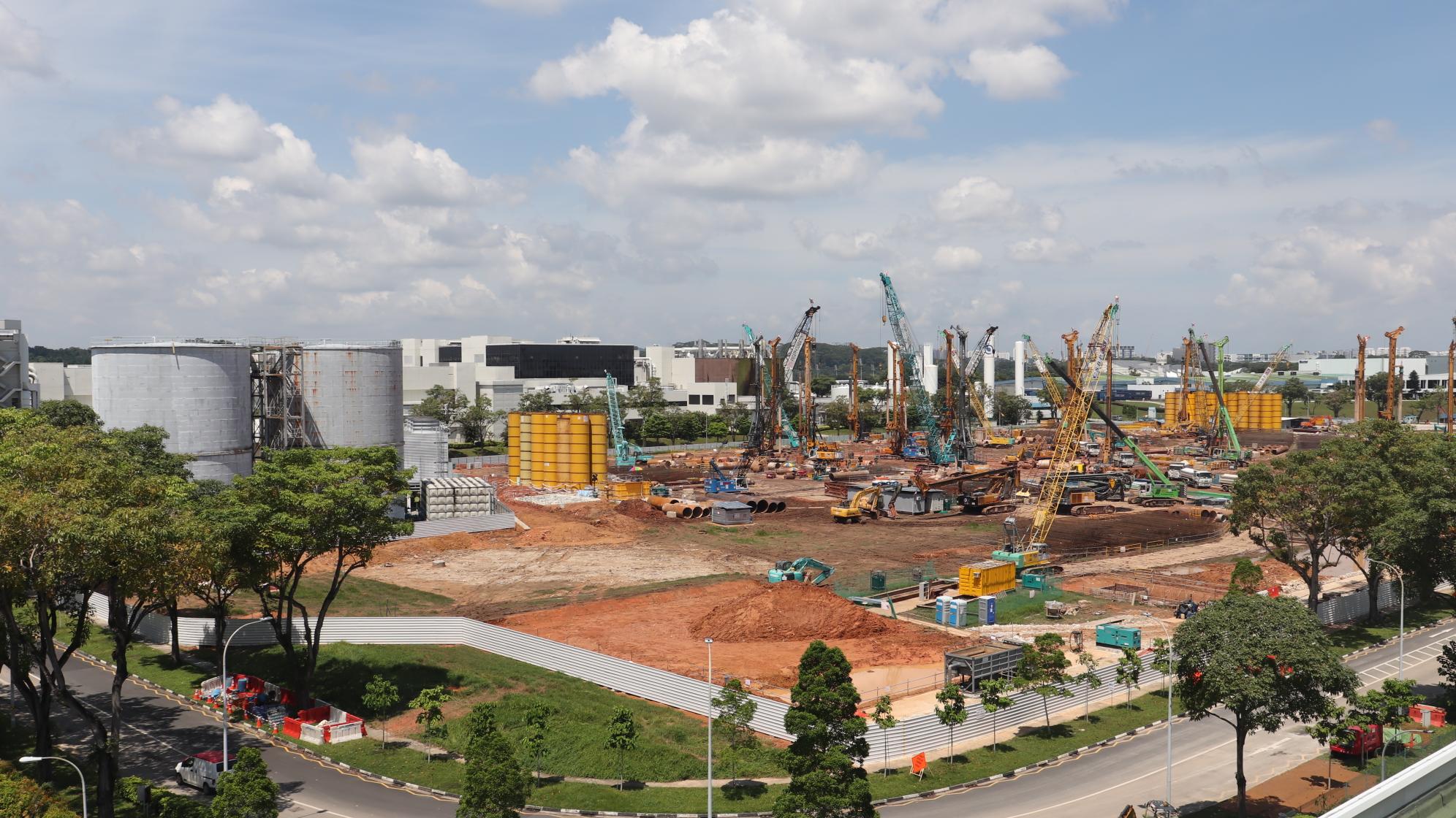
Looking to capitalize on the ongoing chip crunch, GlobalFoundries this morning is announcing that the company is building a new chip fab in Singapore, with the groundbreaking taking place immediately. The unnamed fab will be joining the company’s existing cluster of fabs in Singapore, and once fully ramped up in late 2023, will be capable of processing 450K 300mm wafers per year. The fab is the first of a larger, three phase plan for the foundry, which with investments from customers and the Singapore government, will be spending $4 billion to construct the new fab.
Like the rest of the chip lithography industry, GlobalFoundries is currently enjoying a booming market where they can’t make chips fast enough to satisfy customer demand. Even with multiple fabs located in Singapore, Dresden, and the US, the company is running at capacity and could be selling more chips if they could make them. To that end, the company is preparing to make the first of several planned capacity expansions, starting with its fab cluster in Singapore.
Keeping in line with GlobalFoundries’ pivot towards more specialized processes for specific classes of chips, the new fab is going to be focused on larger process nodes. GloFo is principally investing in capacity for their automotive, 5G mobility and secure device customers, which means adding capacity for their 55nm BiCMOS process for RF, as well as their 40nm processes for embedded memory and RF. A small part of the fab’s capacity is also being set aside for 90nm. And, since this fab is being built with modern tools, the company is being quick to emphasize that these allocations aren’t static, and that many of their tools are fungible, allowing them to be moved between different lines as dictated by demand.
Owing to the unique processes being employed and the overall chip crunch – which even after it diminishes isn’t expected to fully abate any time soon – GloFo is fast-tracking the development of this new fab. With construction already underway (and the formal groundbreaking set for today), the company expects the fab to produce its first commercial wafers in early 2023, only around 18 months from now. And by the time the fab is fully ramped up at the end of 2023, the 250,000 square feet of clean room space will be capable of processing 450K wafers per year (~38K/month). Overall, this marks a nearly 50% increase in GloFo Singapore’s capacity, bringing the total capacity for operations there to 1.5M 300mm wafers per year.
Funding for the $4 billion fab, in turn, is coming from a few sources. According to GlobalFoundries, part of the funding for the fab is coming directly from customers, who are pre-paying for the capacity. As well, Singapore’s Economic Development Board is being listed as a partner. And finally, with GlobalFoundries easily turning a profit, the company has much easier access to loans and other forms of borrowing than it has in previous years.
Overall, this marks the next step in an important turnaround for the contract fab, which was spun-off from AMD almost 13 years ago. Though GlobalFoundries’ plans to compete as a bleeding-edge fab eventually fell to the wayside thanks to the ever-increasing costs of R&D, the company has found a new role as a large-scale provider of older and more specialized manufacturing processes. As a result, GloFo is finally a financially successful chip fab, and with that success comes the need to expand. Once finished, the new Singapore fab will be the first brand-new (and not acquired) fab to be built by the company in several years.
Meanwhile, Singapore is just the first of several planned additions for the contract chip fab. Mindful of the current political climate and every major nation’s desire to secure local chip manufacturing capacity, the company is aiming to expand capacity in all three of its fab sites, ideally splitting capacity equally between Singapore, the US, and Dresden. Singapore, in turn, has become the first major expansion on the basis of need – it’s the oldest fab complex and the first to run out of room – but it won’t be the last. GloFo is already in the middle of its previously-announced $1.4B capacity expansion across all of its sites, and the company wants to invest upwards of 6 billion dollars more over the next couple of years. So, as GlobalFoundries’ fortunes continue to rise, so will the additional fab capacity needed to support the company.
Source: GlobalFoundries


5 Comments
View All Comments
Fulljack - Tuesday, June 22, 2021 - link
lucky for Singapore, while very limited in land area, they got all the high-paying technology companies there. I guess their development are very critical to compete against neighboring Asean countries.milli - Tuesday, June 22, 2021 - link
"Overall, this marks the next step in an important turnaround for the contract fab, which was spun-off from AMD almost 13 years ago."Though I think that this specific expansion has more to do with the ashes of Chartered Semiconductor than AMD.
Yojimbo - Tuesday, June 22, 2021 - link
Aren't the ashes of AMD going completely cold since they stopped development of leading edge semiconductor nodes?Oxford Guy - Friday, June 25, 2021 - link
Still have a working 90nm Sempron machine with a massive 2 GB of DDR1 400. Cheap ECS board.90nm certainly isn’t very exciting. 32nm is very old. 90nm is very ancient.
At some point it seems like a waste of silicon to use such large processes. I would have thought 28nm ‘bulk’ would be cheap enough by now to mostly relegate larger lithography to the EOL bracket. 40nm I can see, though. 90nm seems rather sad.
Perhaps it’s the design rules complexity (which increases with shrinkage according to a TSMC tech) that holds that back, not just higher equipment cost. Or, is equipment availability the biggest problem in terms of more recent but hardly cutting-edge stuff? My questions were probably answered in articles here that I missed. I know people will say that the ancient nodes are good enough for this and that but surely 28nm would be both good enough and require less silicon per chip.
So, clearly the cost of silicon wafers is a small component. Wafer-scale for the masses then. : ) Let’s use old nodes to bring the price way down for a wafer-scale GPU.
SemiChemE - Sunday, July 11, 2021 - link
At least three factors account for the continued use of older nodes:1. Legacy products - It's much cheaper and more reliable to continue to use an existing design, especially one that already has a long history than to spin and requalify a new design. This is especially true for Automotive applications, where reliability is more important than performance.
2. Design costs - As you mentioned, design costs increase at smaller nodes. Thus, for a low-volume product, the design costs can dominate and restrict you to an older node.
3. Device integration (eg. Analog, RF, PA's or other non-logic devices) - many non-logic device types do not really scale, so if a design has a lot of these non-scaling devices you don't see much benefit scaling the logic portion to a smaller and thus more expensive node.