Samsung Announces 'Shinebolt' HBM3E Memory: HBM Hits 36GB Stacks at 9.8 Gbps
by Ryan Smith on October 20, 2023 2:00 PM EST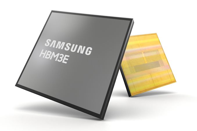
Samsung’s annual Memory Tech Day is taking place in San Jose this morning, and as part of the event, the company is making a couple of notable memory technology announcements/disclosures. The highlight of Samsung’s event is the introduction of Shinebolt, Samsung’s HBM3E memory that will set new marks for both memory bandwidth and memory capacity for high-end processors. The company is also disclosing a bit more on their GDDR7 memory, which will mark a significant technological update to the GDDR family of memory standards.
Starting things off, we have today’s marquee announcement: Shinebolt HBM3E memory. Like the rest of the memory industry, Samsung is preparing a successor to the current-generation of HBM3 memory that’s being used with high-end/HPC-grade processors, with the industry settling around the upcoming HBM3E standard. HBM3E is slated to offer both significantly higher capacities and greater memory bandwidth than HBM3, helping the high-bandwidth memory technology keep up with ever-growing workloads on high-end processors.
| Samsung HBM Memory Generations | ||||||
| HBM3E (Shinebolt) |
HBM3 (Icebolt) |
HBM2E (Flashbolt) |
HBM2 (Aquabolt) |
|||
| Max Capacity | 36GB | 24 GB | 16 GB | 8 GB | ||
| Max Bandwidth Per Pin | 9.8 Gb/s | 6.4 Gb/s | 3.6 Gb/s | 2.0 Gb/s | ||
| Number of DRAM ICs per Stack | 12 | 12 | 8 | 8 | ||
| Effective Bus Width | 1024-bit | |||||
| Voltage | ? | 1.1 V | 1.2 V | 1.2 V | ||
| Bandwidth per Stack | 1.225 TB/s | 819.2 GB/s | 460.8 GB/s | 256 GB/s | ||
The basis of Shinebolt is a new 24Gbit HBM memory die, which Samsung will be producing on their D1a process, the company’s EUV-based 4th generation 10nm-class (14nm) node. Samsung will be producing both 8Hi and eventually 12Hi stacks based on this new die, allowing for total stack capacities of 24GB and 36GB respectively, 50% more capacity than their HBM3 (Icebolt) equivalents.
According to Samsung, Shinebolt will be able to hit memory clockspeeds as high as 9.8Gbps/pin, better than 50% faster than their HBM3 products. Though given some of Samsung’s previous memory clockspeed claims, there’s a good chance this is a semi-overclocked state. Shinebolt development isn’t far enough along for Samsung to list individual SKUs, but even at the conservative end of things, Samsung is promoting data rates of at least 8Gbps/pin in their event press release. And if Samsung’s ambitious memory frequencies do come to fruition, then that would put Samsung ahead of their competition as well; to date, SK hynix and Micron have announced plans for 9Gbps/pin and 9.2Gbps/pin memory respectively, so Samsung’s claims are certainly the most aggressive.
Overall, these clockspeeds would give a single HBM3E stack a minimum bandwidth of 1TB/sec, and a maximum bandwidth of 1.225TB/sec, well ahead of the 819GB/sec data rate of HBM3. Or to frame things in reference of a high-end processor (e.g. NVIDIA H100), a 6-stack chip would be able to access as much as 216GB of memory with an aggregate memory bandwidth as high as 7.35TB/sec.
As for power efficiency, things look to be a bit of a mixed bag. On a relative basis, Samsung says that Shinebolt will be 10% more efficient than Icebolt – in other words, consuming 10% less power per bit transferred (pJ/bit). However, a 25%+ clockspeed improvement will more than wipe out those gains due to the significant increase in bits transferred. So while Shinebolt will be more efficient overall, on an absolute basis it seems that total power consumption for HBM memory will continue to grow with the next generation.
Either way, for the high-end processor market that Samsung is targeting with Shinebolt, chipmakers are unlikely to be fazed by the power increase. Like the rest of the high-end processor space, Samsung has the AI market set square in its sights – a market segment where both memory bandwidth and memory capacity are limiting factors, especially with massive large language models (LLMs). Along with the traditional supercomputer and networking market segments, Samsung should have little trouble selling faster HBM in the middle of a booming AI market.
Like the other major memory vendors, Samsung expects to ship Shinebolt at some point in 2024. Given that the company just started sampling the memory – and that HBM3 Icebolt itself just hit mass production – Shinebolt’s likely not shipping until the later part of the year.
A Brief Teaser on HBM4: FinFETs & Copper-to-Copper Bonding
Finally, looking even farther into the future, Samsung is briefly talking about their plans for HBM4 memory. While that technology is still a few years off (there’s not even an approved specification for it yet), we know from previous disclosures that the memory industry is aiming to move to a wider, 2048-bit memory interface. Which, as Samsung likes to frame things, is the only practical choice when further HBM clockspeed increases would blow out power consumption.
For HBM4, Samsung is looking at employing more advanced fab and packaging technologies that are currently the domain of logic chips. On the fab side of matters, the company wants to move to using FinFET transistors for their memory, as opposed to the planar transistors still used there. As with logic, FinFETs would reduce the drive current required, which would help to improve DRAM energy efficiency. Meanwhile on the packaging side of matters, Samsung is looking at moving from micro-bump bonding to bumpless (direct copper-to-copper) bonding, a packing technique that’s still on the cutting-edge of development even in the logic space. Embracing cutting-edge technologies will be critical to keeping HBM bandwidth growing as it has over the last decade, but the costs and complexities of doing so also underscore why HBM remains an exclusively niche high-end memory technology.
GDDR7 Update: 50% Lower Stand-By Power Than GDDR6
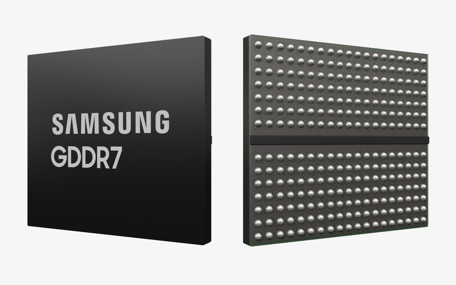
Besides HBM3E, Samsung’s other big bandwidth memory update of the day is a brief status update on their GDDR7 memory.
Back in July of this year, Samsung announced that they completed initial development on their GDDR7 memory. The next generation of GDDR memory, GDDR7 brings with it several major changes versus today’s GDDR6, the most significant of which is a switch to PAM3 encoding. PAM3 allows for 1.5 bits to be transferred per cycle (or rather 3 bits over two cycles), opening the door to improving memory transfer rates without employing more costly means of further improving the frequency of the memory bus.
| GDDR Memory Generations | |||||
| GDDR7 | GDDR6X | GDDR6 | |||
| B/W Per Pin | 32 Gbps (Projected) | 24 Gbps (Shipping) | 24 Gbps (Sampling) | ||
| Chip Density | 2 GB (16 Gb) | 2 GB (16 Gb) | 2 GB (16 Gb) | ||
| Total B/W (256-bit bus) | 1024 GB/sec | 768 GB/ssec | 768 GB/ssec | ||
| DRAM Voltage | 1.2 V | 1.35 V | 1.35 V | ||
| Data Rate | QDR | QDR | QDR | ||
| Signaling | PAM-3 | PAM-4 | NRZ (Binary) | ||
| Packaging | 266 FBGA | 180 FBGA | 180 FBGA | ||
As a quick recap from Samsung’s July announcement, Samsung will be rolling out 16Gbit (2GB) modules, which will be able to run at up to 32Gbps/pin. That’s a 33% improvement in bandwidth per pin over current GDDR6 memory, and would bring the aggregate bandwidth of a 256-bit memory bus to a cool 1TB/second. GDDR7 should also deliver a 20% improvement in power efficiency over Samsung’s GDDR6 (in terms of pJ/bit), thanks in part to the use of Samsung’s 3rd generation D1z (10nm-class) fab node.
Today’s event from Samsung is largely a recap of July’s announcement, but in the process we have learned a couple of new technical details on GDDR7 that Samsung hasn’t previously disclosed. First off, GDDR7 isn’t just improving active power consumption, but the tech will also improve on stand-by power consumption to a significant degree. Thanks to additional clock controls, GDDR7 will consume 50% less stand-by power than GDDR6.
Second, in discussing why Samsung (and the industry as a whole) went with PAM3 encoding for GDDR7 instead of even denser PAM4, the company confirmed some of our technical suppositions on the new technology. In short, PAM3 has a lower average bit error rate (BER) than PAM4, largely thanks to the wider margins on the eye window. None of which makes PAM4 unworkable (as Micron has already proven), but Samsung and the rest of the memory industry are favoring the relative simplicity of PAM3, given the trade-offs.
Besides the usual video card/gaming customers, Samsung is expecting GDDR7 to be adopted by AI chip makers, and perhaps a bit more surprisingly, the automotive industry. In fact some of these non-traditional customers may be the first to adopt the memory; since the traditional GPU vendors are still mid-cycle on their current generation of products, it will still be quite some time before they ship any GDDR7-capable silicon.
At this point Samsung has not announced a projected date for when their GDDR7 memory will go into mass production. But the company is still expecting that they will be the first vendor to ship the next-generation memory, presumably in 2024.
Source: Samsung


10 Comments
View All Comments
Dante Verizon - Friday, October 20, 2023 - link
Why doesn't the chip density increase...meacupla - Saturday, October 21, 2023 - link
probably because it's new technology.Hopefully we get to see 3GB and 4GB densities down the line.
deil - Tuesday, October 24, 2023 - link
stability is an issue at start, going up instantly is unwise. best method we have is tick tock, migrate -> upgrade -> migrate -> upgrade.zepi - Saturday, October 21, 2023 - link
DRAM stores bit state in a capacitor. The smaller (physically) you make the capacitor, the less capacitance it has and the quicker it drains out and needs refreshing. And when you keep scaling down, eventually you have never time to actually read / write data as all you do is refresh the bits.In typical DRAM the density is limited by a layer of hexagonally stored capacitances and the transistors are then manufactured to a separate layer. Increasing density of transistors in the bit-lane layer doesn't really help, because capacitors still need to be kept more or less same size.
That is why DRAM doesn't really scale down with manufacturing process the same way as logic does. Logic chips like CPU's/GPU's are made of (mostly) transistors that don't need to store charge -> can be made infinitely small as long as they act as transistors.
meacupla - Saturday, October 21, 2023 - link
Chip density is not the same as node/capacitor size.For instance, Micron/Crucial has 3Gb density DDR5 and are working on 4Gb. That's how you get their 12GB and 24GB sticks.
Dante Verizon - Saturday, October 21, 2023 - link
I hope so, I would like to see an RX nano 2, or some other compact high-end model. It's a shame HBM never became popular or dropped in price, in terms of efficiency, bandwidth and size it's an incredible solution.Threska - Sunday, October 22, 2023 - link
Maybe nanoimprint may be the solution.https://youtu.be/8UdNB3ZY4Ks
Threska - Friday, October 20, 2023 - link
Interesting although AI may take a different approach.https://www.nature.com/articles/d41586-023-03267-0
rpg1966 - Sunday, October 22, 2023 - link
"PAM3 allows for 1.5 bits to be transferred per cycle (or rather 3 bits over two cycles), opening the door to improving memory transfer rates"I'm clearly missing something obvious here. How does going from GDDR6X's PAM4 to GDDR7's PAM3 improve transfer rates (ignoring the clock speed differences)?
Ryan Smith - Sunday, October 22, 2023 - link
GDDR6X isn't a JEDEC standard, so it's not what's being compared here. Samsung is going from G6 to G7.G7's PAM3 encoding has a lower density than G6X's PAM 4 (1.5b vs 2b). But it'll hit higher clockspeeds and be less complex to implement.