Arm Announces Neoverse N1 & E1 Platforms & CPUs: Enabling A Huge Jump In Infrastructure Performance
by Andrei Frumusanu on February 20, 2019 9:00 AM ESTThe Neoverse E1 CPU: A Small SMT Core for the Data-Plane
We’ve talked a lot about the Neoverse N1 – but today’s announcement actually covers two new platforms. Today actually isn’t the first time that we’ve talked about the other new platform, the new Neoverse E1. Codenamed Helios, the E1 CPU actually is derived from the Cortex-A65AE which we’ve already briefly talked about in December.
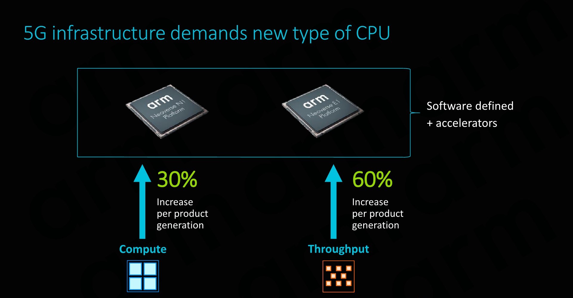
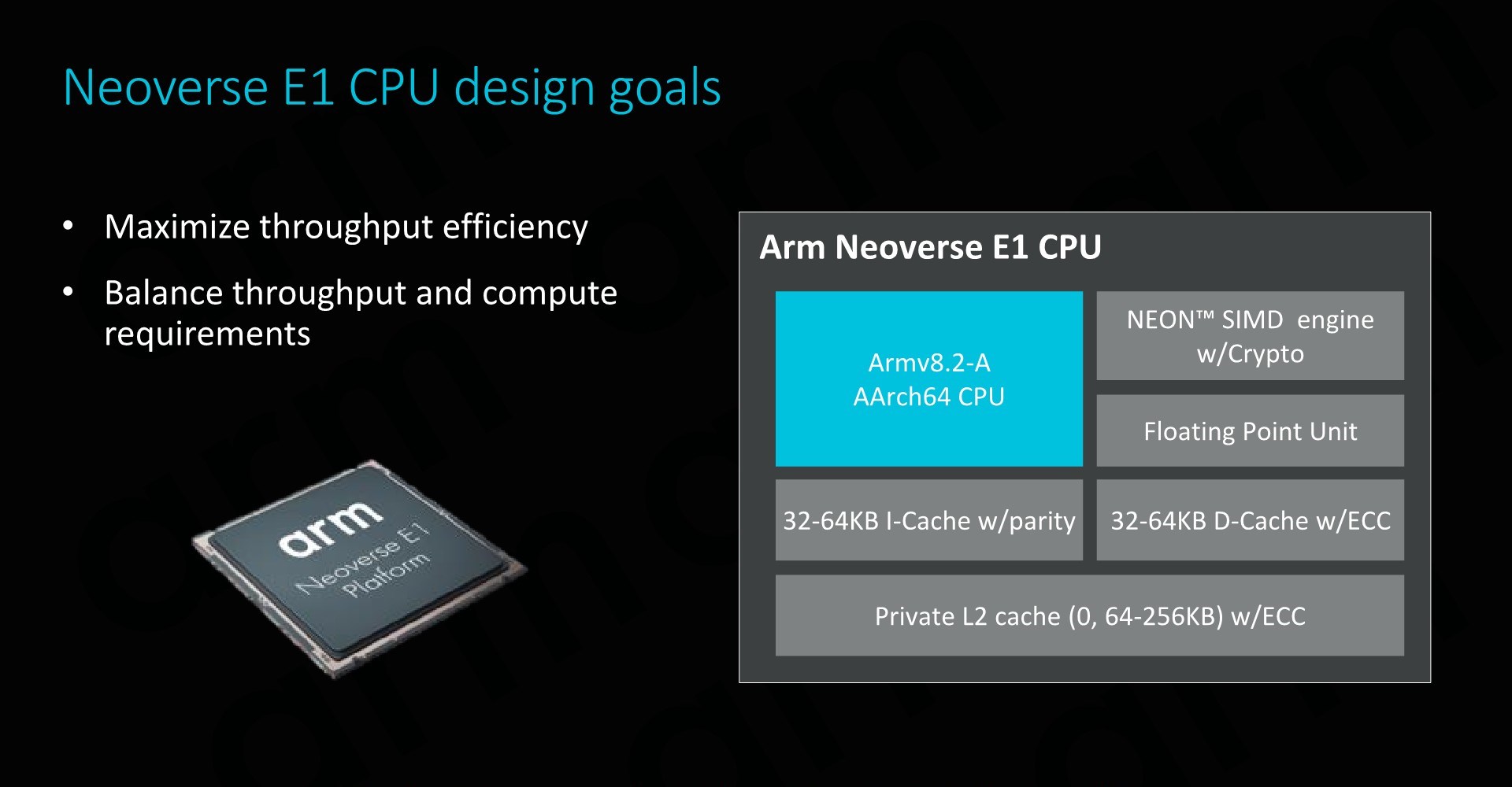
Arm largely differentiates between two big workload types in infrastructure deployments, “Compute” use-cases where we need arithmetically capable CPU cores such as the N1, and “Throughput” workloads that largely are mainly about shifting large amounts of data around. The latter category is what the new Neoverse E1 is targeting, representing a specialised CPU core that efficiently and cost effectively is able to handle such tasks.
Arm’s First SMT Core
As some might have read in the Cortex-A65AE announcement piece, the µarchitecture used in Helios both in the Cortex chip as well as in the Neoverse E1 represents Arm’s first ever foray into designing and bringing to market an SMT (simultaneous multi-threading) core. It may at first glance sound a bit weird to have SMT introduced in a smaller CPU core, as traditionally we would be thinking about SMT being useful in raising the back-end execution unit utilisation rate in larger microarchitectures, but it actually makes a lot of sense as well in smaller CPU cores whose workloads are predominantly in the data plane.
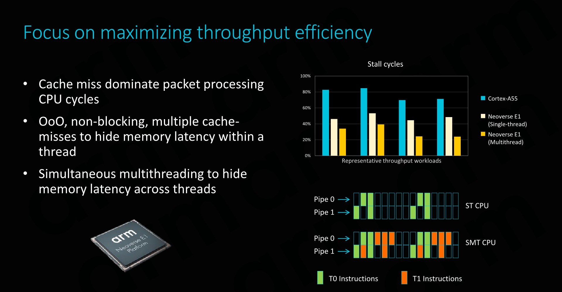
In data-processing workloads, cache misses dominate CPU work cycles. This is because we’re talking about data that inherently doesn’t have a long residence time on the CPU core, either streaming from sensors as described in the use-case of the Cortex-A65AE, or in this case streaming from the network in the case of infrastructure workloads. This means that the CPU has to deal with long memory latency accesses, introducing stalls in the CPU pipelines.
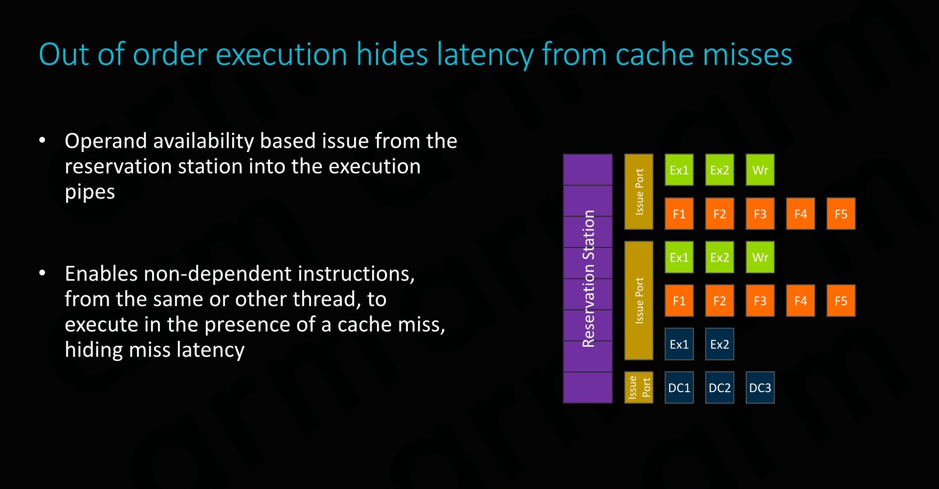
The E1 CPU is a small out-of-order design with SMT: In data-plane heavy workloads, introducing the ability to handle a secondary thread on the CPU core essentially represents almost a free throughput gain for the microarchitecture, as it’s able to fill unused execution cycles that otherwise would have just gone to waste. Indeed in optimal workloads, this can result in essentially a doubling of the throughput, on top of the single-threaded microarchitectural gains that the E1 CPU brings over predecessors such as the Cortex A55.
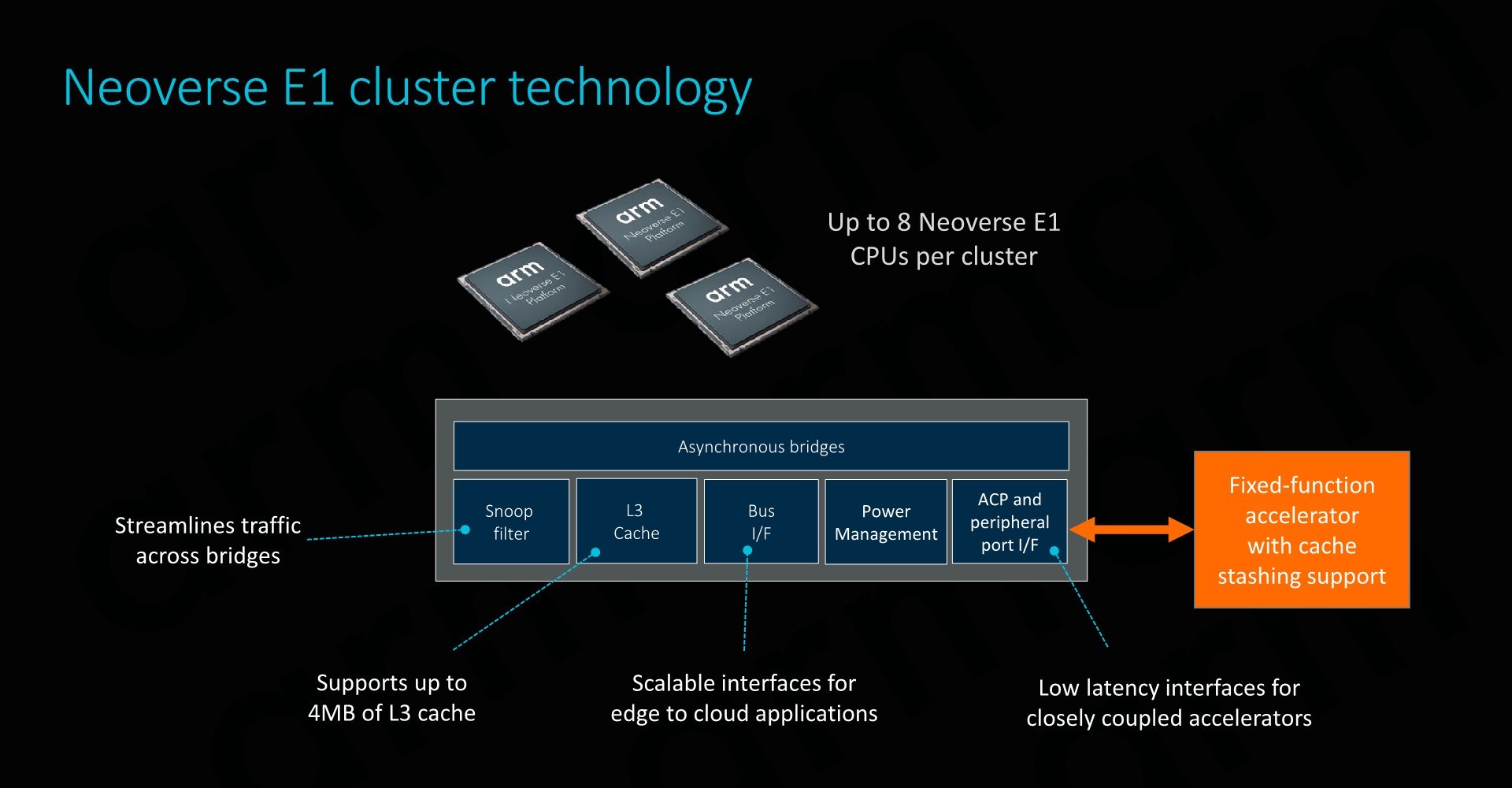
At the cluster level, the Neoverse E1 CPU configuration options are extremely similar to what we’ve seen deployable in DynamIQ systems. The cluster itself looks very much like a DSU, with up to eight cores, a cluster-level snoop filter, and an L3 cache configurable up to 4MB.
The E1 CPU’s Pipelines
The E1’s CPU pipeline actually represents a brand new-design which (besides the A65) haven’t seen employed before. What Arm has done here is take the foundation of what was the in-order Cortex A55 µarch and turned it into a minimally narrow out-of-order CPU. Moving to a basic out-of-order CPU design was essential in order to get more throughput out of the core, as it avoids stalling the whole pipeline in scenarios where we’d have a long load.
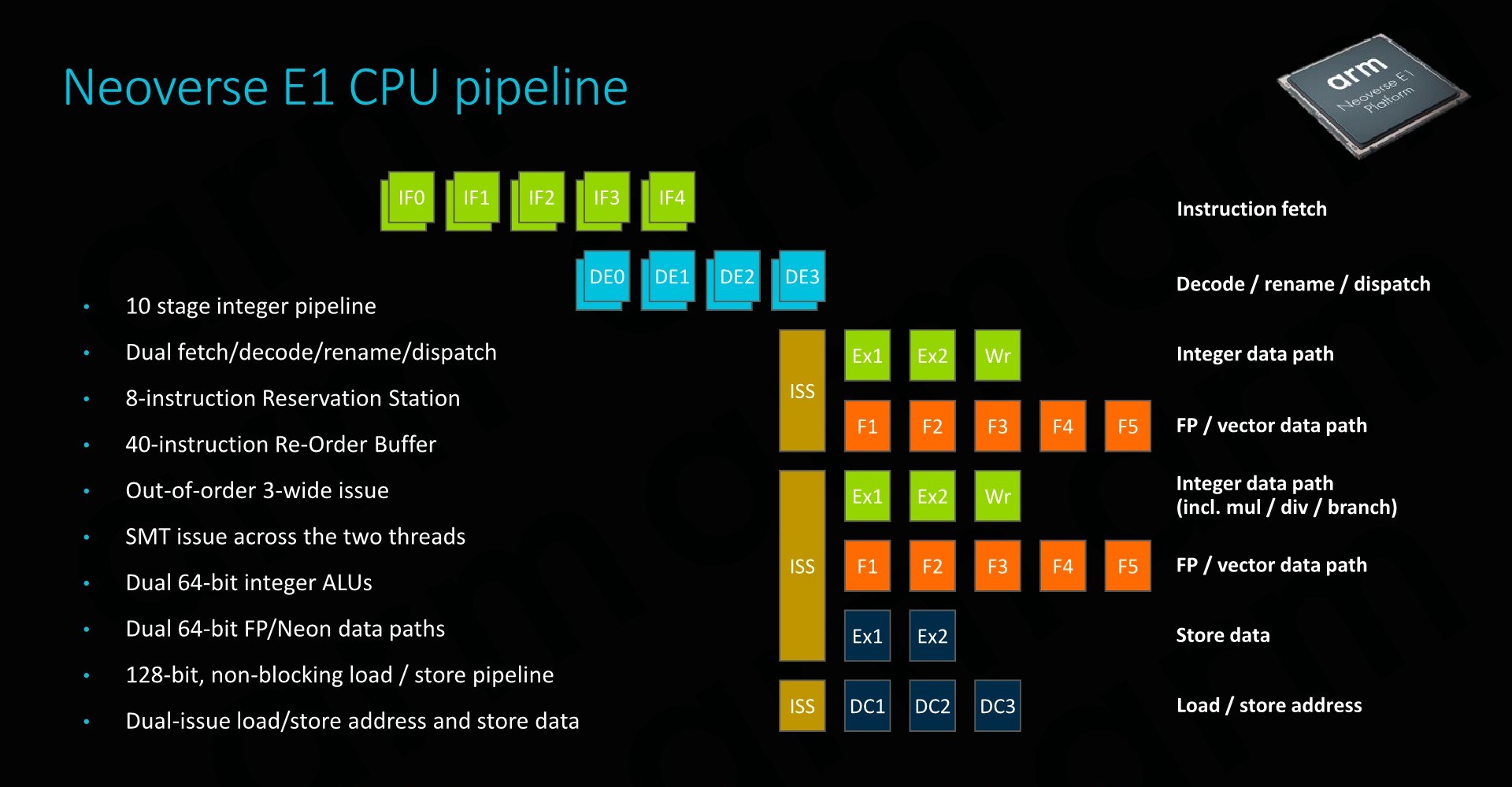
The fetch/decode/dispatch stages of the pipeline is 2-wide. In terms of its out-of-order windows, we see a small 40-deep ROB (Re-order buffer).
On the back-end we find a similar execution unit count and layout as on the Cortex-A55. A big difference to the A55 is that the integer ALUs are now differently partitioned: One ALU is dedicated for simple arithmetic operations only, while the second unit now takes over both integer multiplication as well as division tasks, whereas this was divided among the two ALUs in the A55. Interestingly, Arm also demarks the branch port being shared with this second complex integer ALUs, no longer representing it as a dedicated port as on the A55.
The SIMD/Neon pipelines seem to remain the same as on the A55 in terms of its high-level capabilities, but it is possible Arm may have improved cycle latencies of some instructions between the two generations.
Finally, the load and store ports also match the capabilities of the A55.
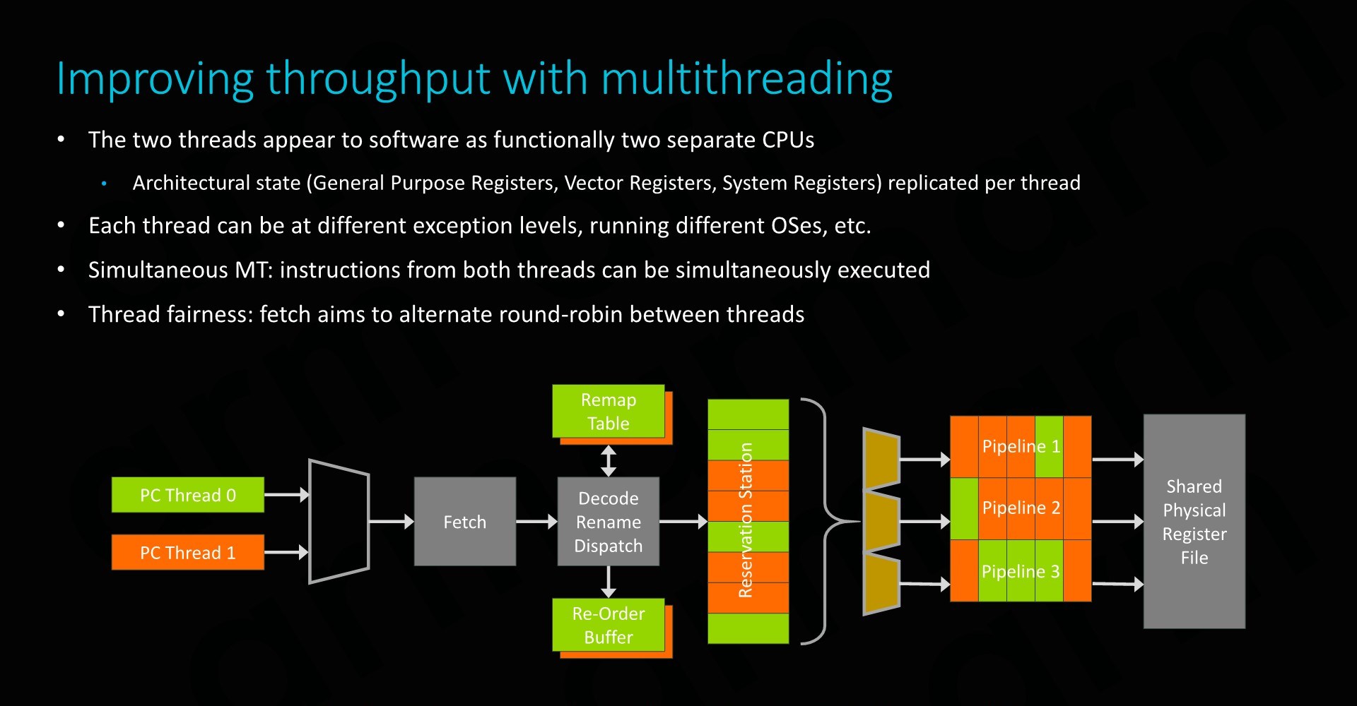
SMT on the Neoverse E1 is enabled through the duplication of architectural state components of the core. This means the CPU has double the general purpose, vector and system registers and their corresponding structures on the physical core.
At the software level, this naturally simply appears as two separate CPU cores, and can be run at different exception levels or even be running different OSes.
Performance partitioning between the two threads is enabled by a simple round-robin instruction fetch mechanism, ensuing that both threads get the same amount of attention.
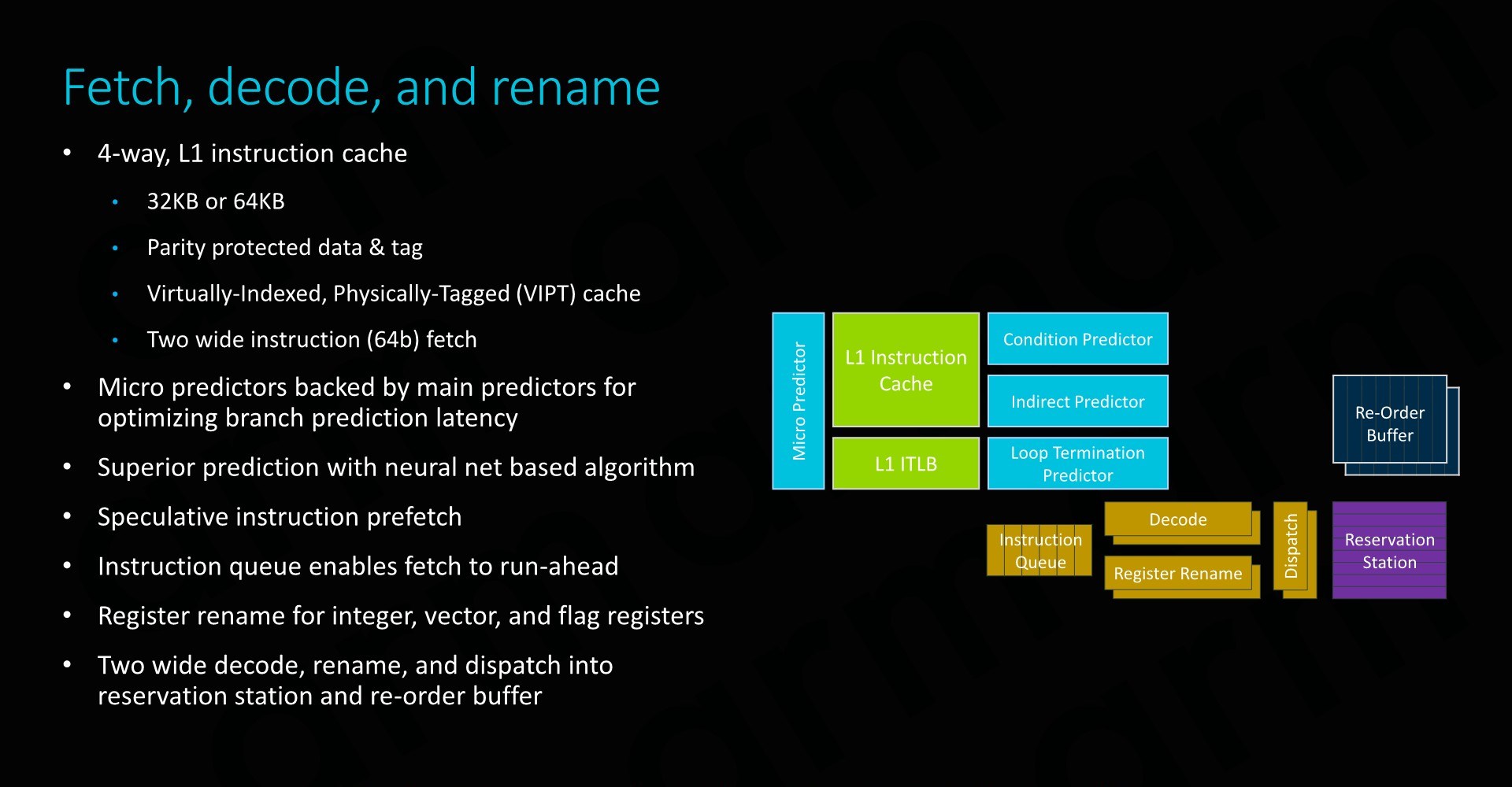
The front-end of the CPU has seen improvements in all regards and adopts many of the state-of-the art front end branch prediction and prefetch mechanisms we find in other more recent Arm OoO cores – just in a more limited implementation optimised for the smaller nature of the E1 CPU.
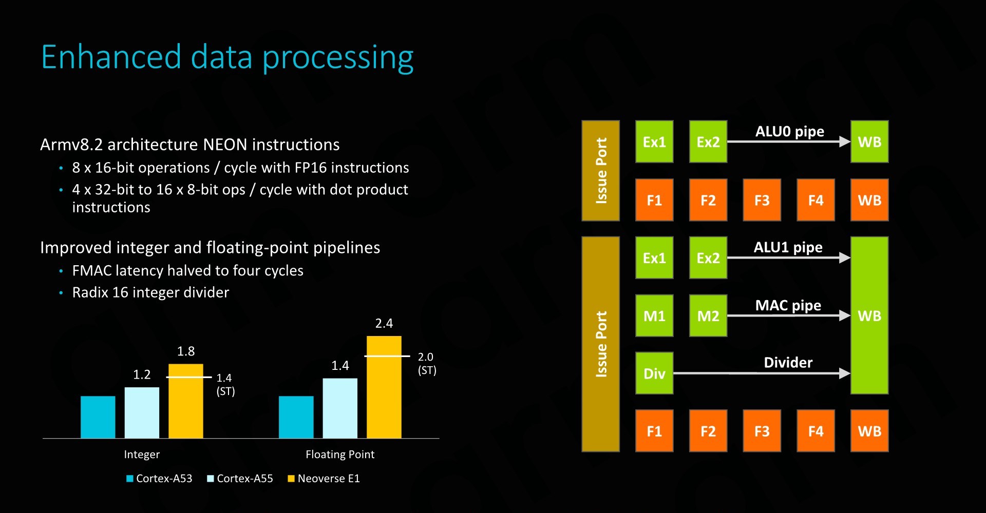
As mentioned just earlier, although the throughput of the execution pipelines hasn’t fundamentally changed, Arm has updated the execution units to employ newer designs with shorter cycle latencies. Here in particular FMAC latency has bene halved, while the integer division unit has been updated to a Radix-16 unit. It’s to be noted that these improvements are again slightly misleading as Arm is making comparisons to the Cortex A53 – the newer Cortex A55 already employed the aforementioned changed, including the new ARMv8.2 double throughput FP16 instructions as well as Int8 dot-products.
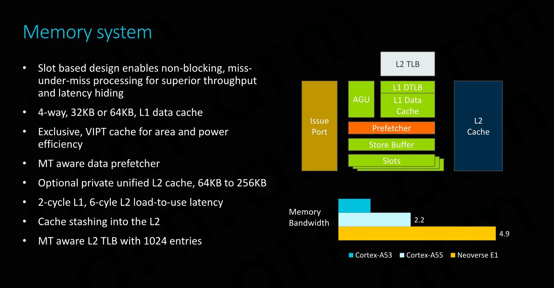
On the memory system side of things, we again see very large similarities to the Cortex A55 and the E1 enjoys the same improvements made by that µarch. The only other notable changes here are the fact that the data prefetchers as well as the L2 TLB are now multi-thread aware and are optimised in their design to better operate with the new SMT nature of the core.


101 Comments
View All Comments
Santoval - Thursday, February 21, 2019 - link
"Both Intel and AMD have been making chips that take the CISC instructions and run them through an instruction decoder that then hands RISC instructions to the actual cpu."The instruction decoder is also part of an "actual CPU". Beside the decoder the front-end also has instruction fetch, a branch predictor, predecode (potentially), μOP & L1 instruction cache, instruction queues, a TLB, allocation queues etc etc All these units are most certainly parts of the "actual CPU".
I believe you rather meant "hands RISC-like instructions to the *back-end* of the CPU".
FunBunny2 - Thursday, February 21, 2019 - link
"The speed advantages on paper between RISC and CISC are in theory a wash. "not to keep beating the dead horse 360, dated as it is, but with the hardware of the time (and IBM was the top of the heap, then) the 360/30 ran the instruction set in micro-code. allegedly the first computer to even have microcode. ran like drek compared to the all-hardware versions of the machine. the '30 real cpu was long reputed to be some DEC machine.
"cpu design quite a bit without being so closely tied to backwards compatibility."
lots of folks say that, but makes no sense to me. compilers target the instruction set, which only changes when Intel publishes 'extensions'. whether those instructions are executed in pure ISA hardware, or a rat running in a spinning wheel (RISC), makes no difference to the compiler writer.
the profiling explanation for microcode over pure ISA hardware makes the most sense.
Wilco1 - Wednesday, February 20, 2019 - link
The only misinformation is from you. RTL simulation is widely used in the industry and is quite accurate.Studies have shown CISC instructions don't do more than RISC instructions - partly because compilers avoid CISC instructions, partly because CISC instructions are slow. That's why RISC works. But I wouldn't expect you to understand this.
FunBunny2 - Thursday, February 21, 2019 - link
"Studies have shown CISC instructions don't do more than RISC instructions "at least in the z world (and predecessors), there were/are some (I don't remember the count) of 'COBOL assist' instructions which were/are quite complex and were introduced to reduce the amount of times the COBOL coders had to 'drop down to assembler'. whether that's still true, I can't say.
DigitalVideoProcessor - Thursday, February 21, 2019 - link
CISC vs. RISC is a debate about instruction decode philosophy and it has almost zero bearing on the performance of a system. CISC machines reduce everything to RISC like operations. Saying one does more than another in a given clock is misinformation.melgross - Thursday, February 21, 2019 - link
Those wars are long over. No modern chip is either pure CISC or RISC. Those are long gone.Calin - Thursday, February 21, 2019 - link
SPECint, SPECfp, ... are "work done tasks" - what your're referring to was "MIPS" (or millions of instructions per second). This performance metric has lost its charm since internally x86 processors no longer use x86 instructions but large bundles of microoperations that are done in parallel and can be interleaved (so two instructions that follow each other are broken into micro operations which are reordered, and might be finalized in a different order).Kevin G - Thursday, February 21, 2019 - link
The thing is that real distinction of CISC vs. RISC is lost in their similar implementations: pipelined OoO parallel execution engines. While CISC encoding may* permit more operations to be contained within a single instruction but at the cost of having to decode that instruction into an optimal arrangement given the hardware. The price paid is in power consumption and complexity which may impact factors like maximum clock speed. In the era of many core and power limitations, these attributes are the foundation for RISC to have an edge over legacy CISC designs. Not to say that RISC architectures can't leverage instruction decoding either: expanding out the fields for registers to account for the larger rename register space is a simple procedure.Once chips begin parallel execution, the CISC advantage of doing more per instruction really starts to fall apart. The raw amount of work being done per cycle approaches the common limit of just how much parallelism can be extracted by an inherently serial stream of instructions. Arguably CISC designs can hit this sooner in terms of raw instruction count as the instruction stream is _effectively_ compressed compared to RISC.
*The concept of fused-multiply add instructions was an early staple of RISC architectures. Technically it goes against the purest ideal but traditional RISC designs permitted the number of operands in their instruction formatting to pull this off so they took advantage of an easy performance boost. x86 didn't gain this capability until AVX2 a few years ago.
peevee - Tuesday, February 26, 2019 - link
"I think you are forgetting the very nature of RISC (Arm) vs CISC (x86) architectures"This distinction does not exist in practice for decades.
wumpus - Wednesday, February 20, 2019 - link
It also shows a result showing Zen roughly half the performance of Intel, something that implies a fairly contrived situation. FX8350 might have had half (or worse) than Intel, but Zen is another story.I'm guessing that this involves AVX256 (or higher) specifically optimized for Intel (note that going to AVX512 is only a modest increase since the clockrate is brutally lowered to compensate for the increased power load. Also note that Zen2 (EPYC2 and Ryzen3000) will include native AVX256 execution paths).