Arm Announces Neoverse N1 & E1 Platforms & CPUs: Enabling A Huge Jump In Infrastructure Performance
by Andrei Frumusanu on February 20, 2019 9:00 AM ESTThe Neoverse E1 CPU: A Small SMT Core for the Data-Plane
We’ve talked a lot about the Neoverse N1 – but today’s announcement actually covers two new platforms. Today actually isn’t the first time that we’ve talked about the other new platform, the new Neoverse E1. Codenamed Helios, the E1 CPU actually is derived from the Cortex-A65AE which we’ve already briefly talked about in December.
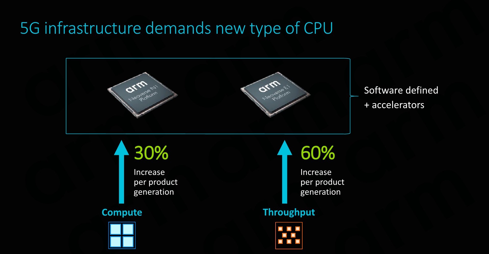
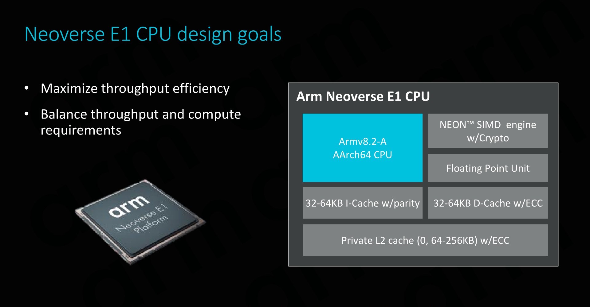
Arm largely differentiates between two big workload types in infrastructure deployments, “Compute” use-cases where we need arithmetically capable CPU cores such as the N1, and “Throughput” workloads that largely are mainly about shifting large amounts of data around. The latter category is what the new Neoverse E1 is targeting, representing a specialised CPU core that efficiently and cost effectively is able to handle such tasks.
Arm’s First SMT Core
As some might have read in the Cortex-A65AE announcement piece, the µarchitecture used in Helios both in the Cortex chip as well as in the Neoverse E1 represents Arm’s first ever foray into designing and bringing to market an SMT (simultaneous multi-threading) core. It may at first glance sound a bit weird to have SMT introduced in a smaller CPU core, as traditionally we would be thinking about SMT being useful in raising the back-end execution unit utilisation rate in larger microarchitectures, but it actually makes a lot of sense as well in smaller CPU cores whose workloads are predominantly in the data plane.
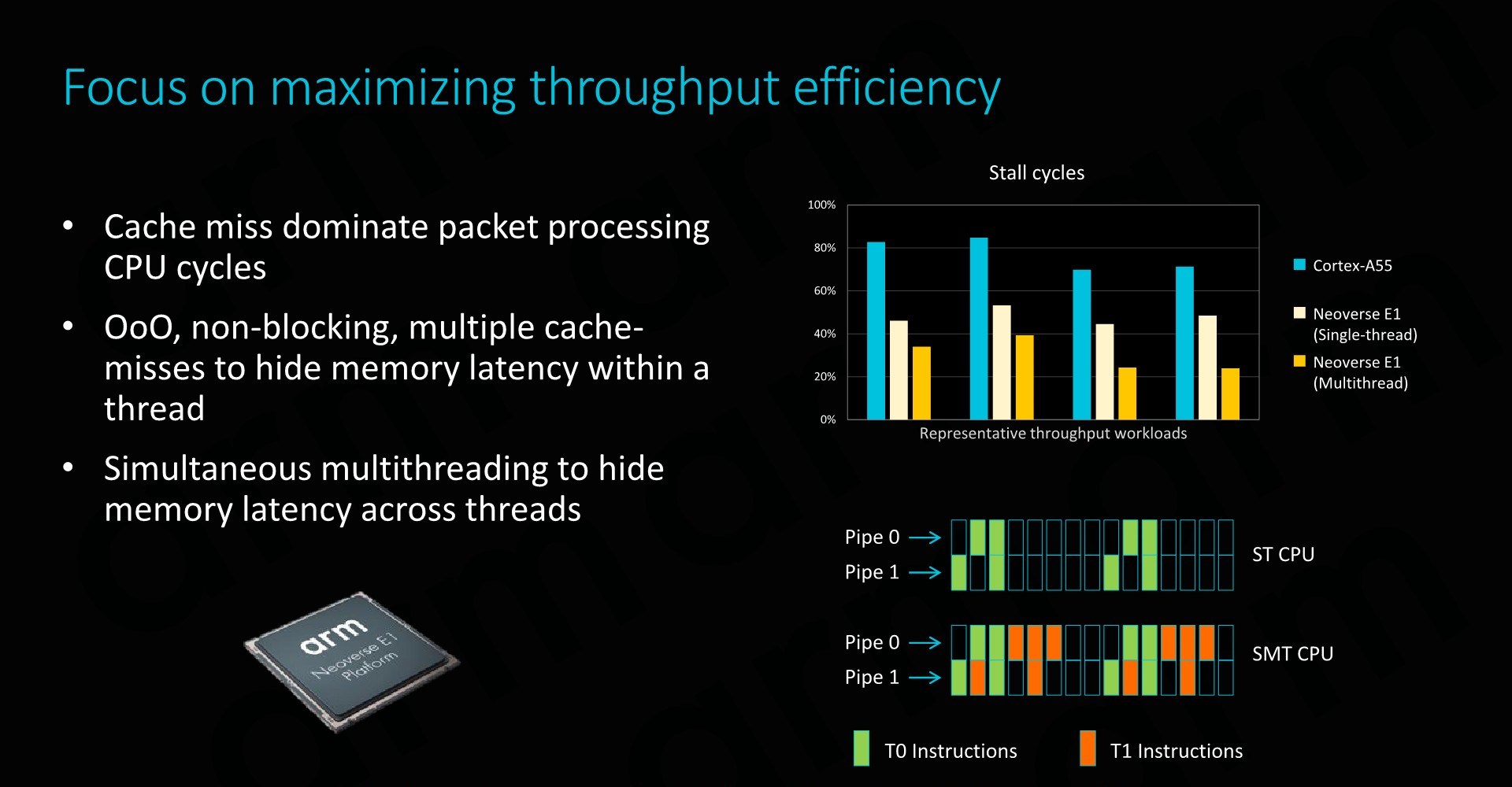
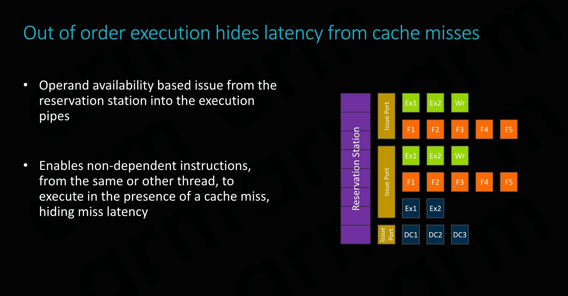
In data-processing workloads, cache misses dominate CPU work cycles. This is because we’re talking about data that inherently doesn’t have a long residence time on the CPU core, either streaming from sensors as described in the use-case of the Cortex-A65AE, or in this case streaming from the network in the case of infrastructure workloads. This means that the CPU has to deal with long memory latency accesses, introducing stalls in the CPU pipelines.
The E1 CPU is a small out-of-order design with SMT: In data-plane heavy workloads, introducing the ability to handle a secondary thread on the CPU core essentially represents almost a free throughput gain for the microarchitecture, as it’s able to fill unused execution cycles that otherwise would have just gone to waste. Indeed in optimal workloads, this can result in essentially a doubling of the throughput, on top of the single-threaded microarchitectural gains that the E1 CPU brings over predecessors such as the Cortex A55.
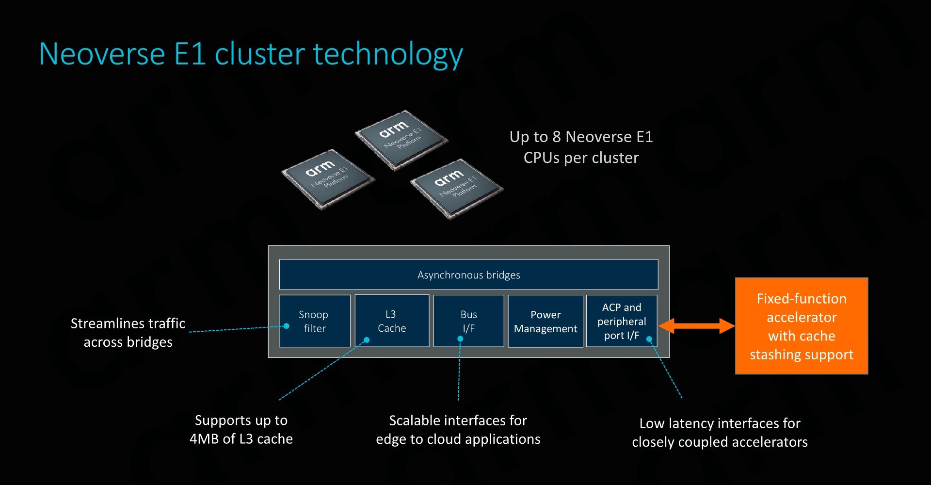
At the cluster level, the Neoverse E1 CPU configuration options are extremely similar to what we’ve seen deployable in DynamIQ systems. The cluster itself looks very much like a DSU, with up to eight cores, a cluster-level snoop filter, and an L3 cache configurable up to 4MB.
The E1 CPU’s Pipelines
The E1’s CPU pipeline actually represents a brand new-design which (besides the A65) haven’t seen employed before. What Arm has done here is take the foundation of what was the in-order Cortex A55 µarch and turned it into a minimally narrow out-of-order CPU. Moving to a basic out-of-order CPU design was essential in order to get more throughput out of the core, as it avoids stalling the whole pipeline in scenarios where we’d have a long load.
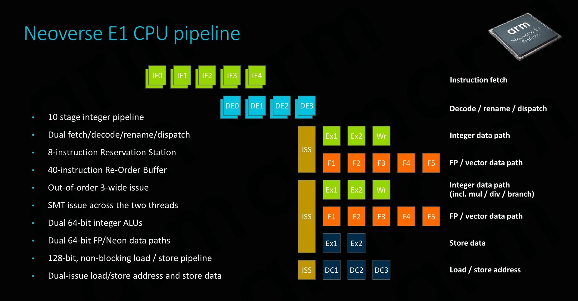
The fetch/decode/dispatch stages of the pipeline is 2-wide. In terms of its out-of-order windows, we see a small 40-deep ROB (Re-order buffer).
On the back-end we find a similar execution unit count and layout as on the Cortex-A55. A big difference to the A55 is that the integer ALUs are now differently partitioned: One ALU is dedicated for simple arithmetic operations only, while the second unit now takes over both integer multiplication as well as division tasks, whereas this was divided among the two ALUs in the A55. Interestingly, Arm also demarks the branch port being shared with this second complex integer ALUs, no longer representing it as a dedicated port as on the A55.
The SIMD/Neon pipelines seem to remain the same as on the A55 in terms of its high-level capabilities, but it is possible Arm may have improved cycle latencies of some instructions between the two generations.
Finally, the load and store ports also match the capabilities of the A55.
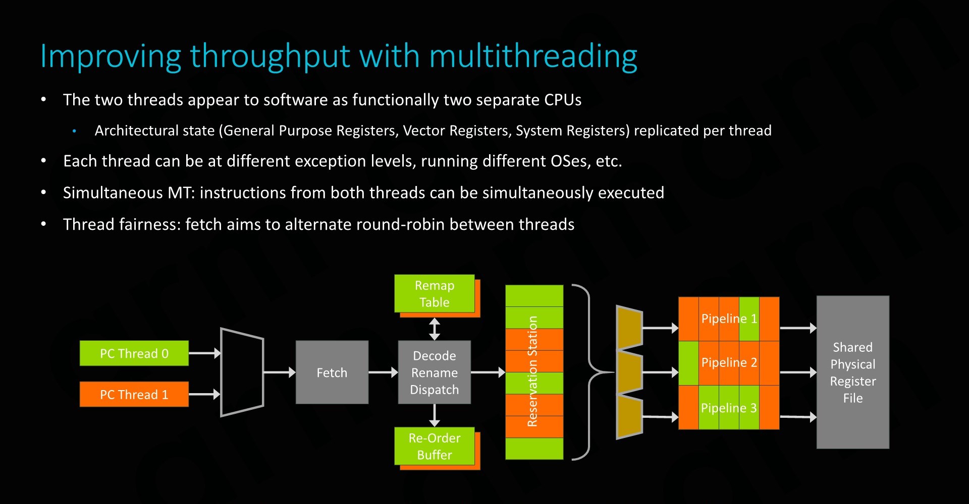
SMT on the Neoverse E1 is enabled through the duplication of architectural state components of the core. This means the CPU has double the general purpose, vector and system registers and their corresponding structures on the physical core.
At the software level, this naturally simply appears as two separate CPU cores, and can be run at different exception levels or even be running different OSes.
Performance partitioning between the two threads is enabled by a simple round-robin instruction fetch mechanism, ensuing that both threads get the same amount of attention.
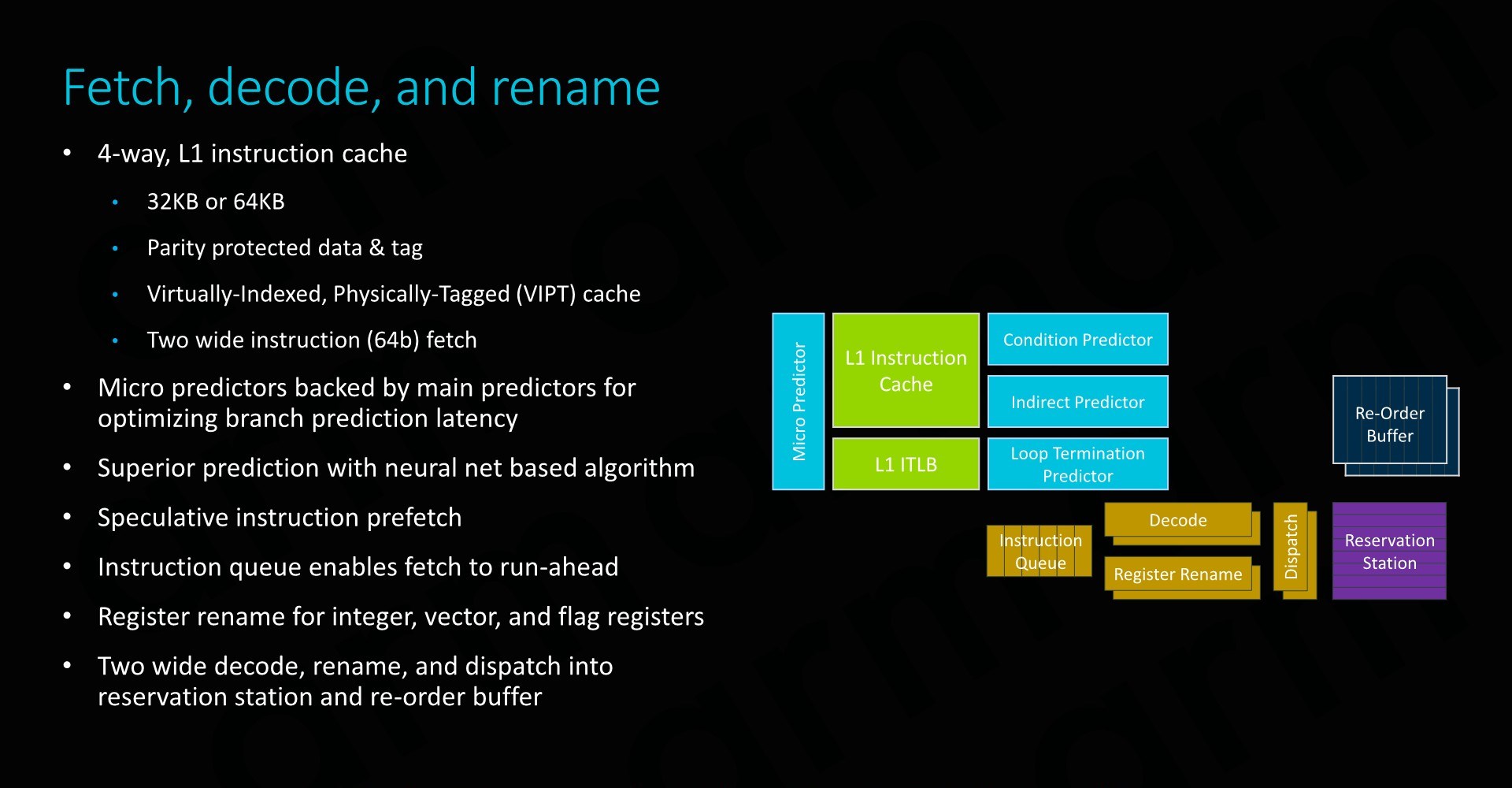
The front-end of the CPU has seen improvements in all regards and adopts many of the state-of-the art front end branch prediction and prefetch mechanisms we find in other more recent Arm OoO cores – just in a more limited implementation optimised for the smaller nature of the E1 CPU.
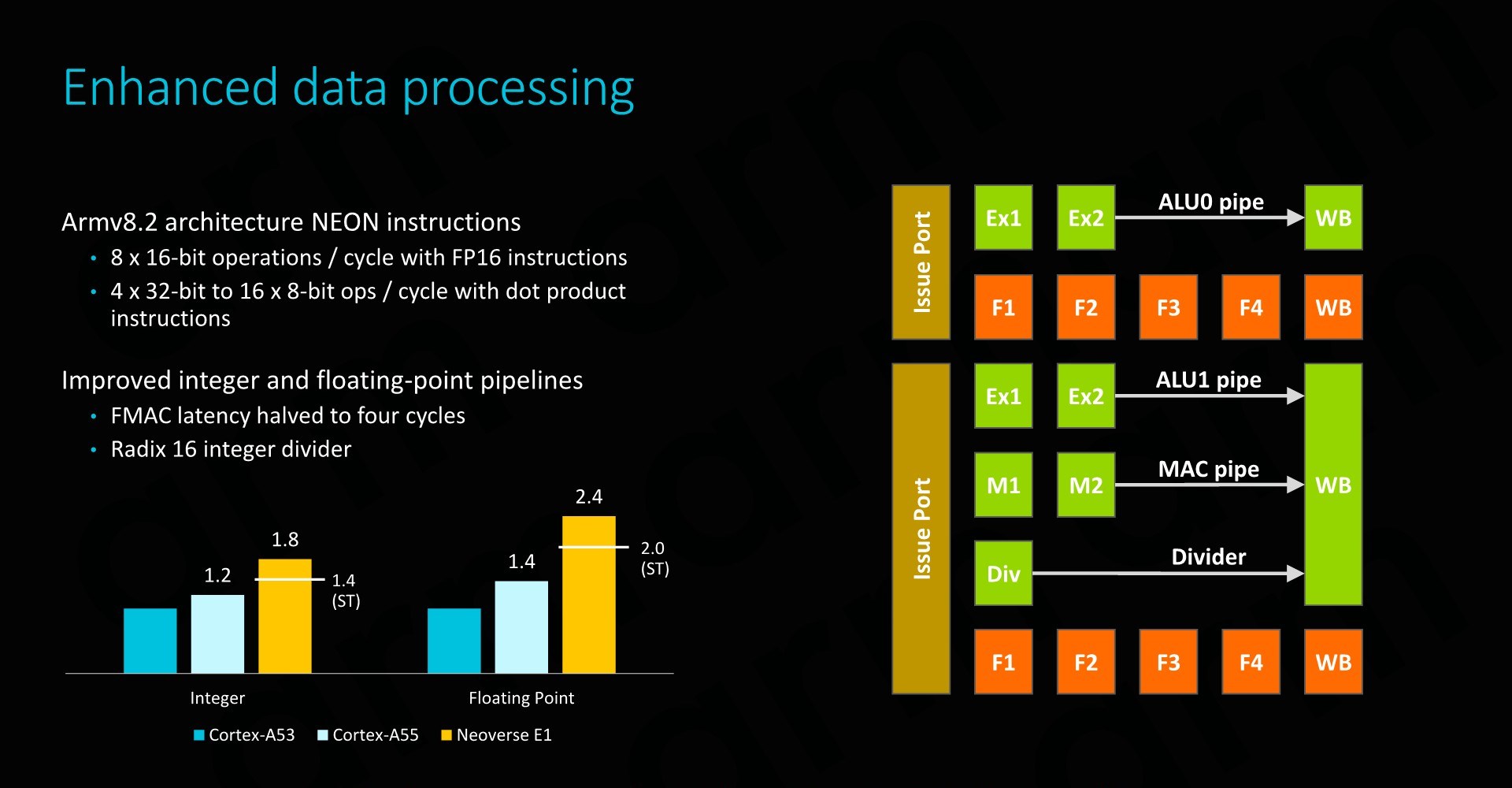
As mentioned just earlier, although the throughput of the execution pipelines hasn’t fundamentally changed, Arm has updated the execution units to employ newer designs with shorter cycle latencies. Here in particular FMAC latency has bene halved, while the integer division unit has been updated to a Radix-16 unit. It’s to be noted that these improvements are again slightly misleading as Arm is making comparisons to the Cortex A53 – the newer Cortex A55 already employed the aforementioned changed, including the new ARMv8.2 double throughput FP16 instructions as well as Int8 dot-products.
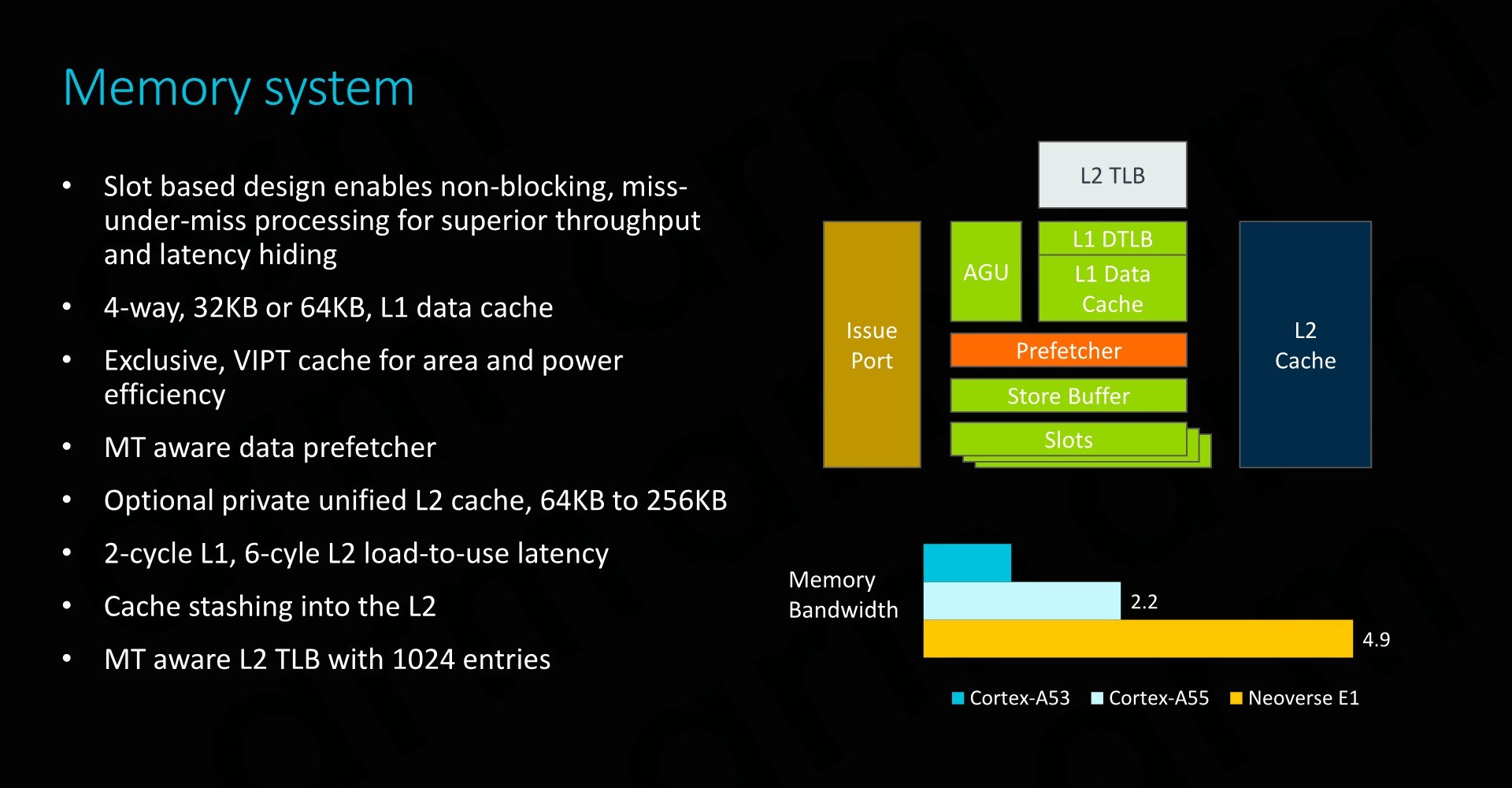
On the memory system side of things, we again see very large similarities to the Cortex A55 and the E1 enjoys the same improvements made by that µarch. The only other notable changes here are the fact that the data prefetchers as well as the L2 TLB are now multi-thread aware and are optimised in their design to better operate with the new SMT nature of the core.


101 Comments
View All Comments
Andrei Frumusanu - Wednesday, February 20, 2019 - link
> It also shows a result showing Zen roughly half the performance of IntelThe W-3175X was at 4.5GHz with the whole 38MB of L3 for the one thread, while the 7601 ran at a peak of 3.2GHz.
Meteor2 - Wednesday, February 20, 2019 - link
I wish you’d normalised for frequency!Andrei Frumusanu - Wednesday, February 20, 2019 - link
That's not the point of the article.ZolaIII - Wednesday, February 20, 2019 - link
Next time read twice before posting. AVX on integer benchmark really?Wilco1 - Wednesday, February 20, 2019 - link
Of course. Never heard of how SIMD hugely affects libquantum for example?Andrei Frumusanu - Wednesday, February 20, 2019 - link
AVX works on integer ...ZolaIII - Wednesday, February 20, 2019 - link
The era of general purpose core's being used for HPC is long time gone. While general purpose core's are hire to stay they will do that with modest number of core's per system, the real push is towards special purpose and multi purpose accelerators. FPGA's being put in the first row because their reprogrammable nature. The ARM actually have an edge over the CISC (X86) because it's simply more efficient which having stellar integer performance for the size of the core. If you look at the development bord it's very clear ARM is pushing into right direction.Meteor2 - Wednesday, February 20, 2019 - link
Kind of. But bottom line is the 20-odd codes used predominantly in the world still run best on general purpose CPUs. Bending software to work on specialised architectures is really hard.ZolaIII - Thursday, February 21, 2019 - link
On the FPGA you bend hardware. That's the whole idea.wumpus - Thursday, February 21, 2019 - link
HPC traditionally meant double precision FLOPS. AI work or similar might want FPGAs until GPUs are sufficiently ready for such things (then FPGA can't keep up).FPGAs are painfully slow at what they do, but can take an entirely new architecture on the fly. We saw that with cryptomining as things went CPU->GPU->FPGA->ASIC. And if you need a lot of multiply-accumulate (like most AI), don't expect anything between GPU and ASIC.