Arm Announces Neoverse N1 & E1 Platforms & CPUs: Enabling A Huge Jump In Infrastructure Performance
by Andrei Frumusanu on February 20, 2019 9:00 AM ESTN1 Hyperscale Reference Design
A big part of what is defining the N1 Platform as an actual platform, is the fact that Arm is offering a full reference design with a set of IPs that is fully validated by Arm themselves.
Here we see three reference designs, a Neoverse N1 hyperscale design, which we’ll get into more detail shortly, an N1 edge design, and a Neoverse E1 edge design. Arm’s goals with the reference designs is to give vendors “sweet-spot” configuration options that they will then be able to implement with (relatively) minimal effort.
The N1 hyperscale design is what we’ll be covering in more detail as this represents Arm’s most cutting-edge and competitive product.
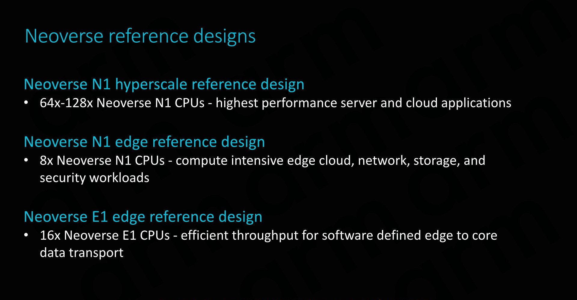
As covered on the previous page, at the heart we find the Neoverse N1 CPU in either 64 or 128 core configurations, integrated in a CMN-600 mesh network with either 64 or 128MB of SLC cache. We also see 128 lanes for PCIe 4 respectively CCIX interfaces which provide plenty of I/O bandwidth.
In terms of memory controllers, Arm employs 8x DD4 interfaces up to 3200MHz. Arm actually has abandoned development of its own memory controllers as customers in most cases opted for their own in-house designs or rather opted to choose IP from other third-party vendors such as Cadence or Synopsys. For the current reference designs Arm’s own DMC-520 was still up-to-date and a well-understood block for the company, although in the future newer memory controllers such as for DDR5 will have to rely on third-party IP. Naturally, the reference design targets the latest 7nm process node.

The physical implementation of the SoC would use replicable hierarchical building blocks for ease of design. A “CPU Tile” consists of the two N1 CPU cores, a slice/bank of the SLC cache as well as part of the CMN’s cross points and home-nodes. This CPU Tile is replicated to generate a “Super Tile”, what is added here is peripheral parts of the SoC such as I/O as well as memory controllers. Finally, replicating the super tile in flipped and mirrored implementations results in the final top-level mesh that is to be implemented on the SoC.
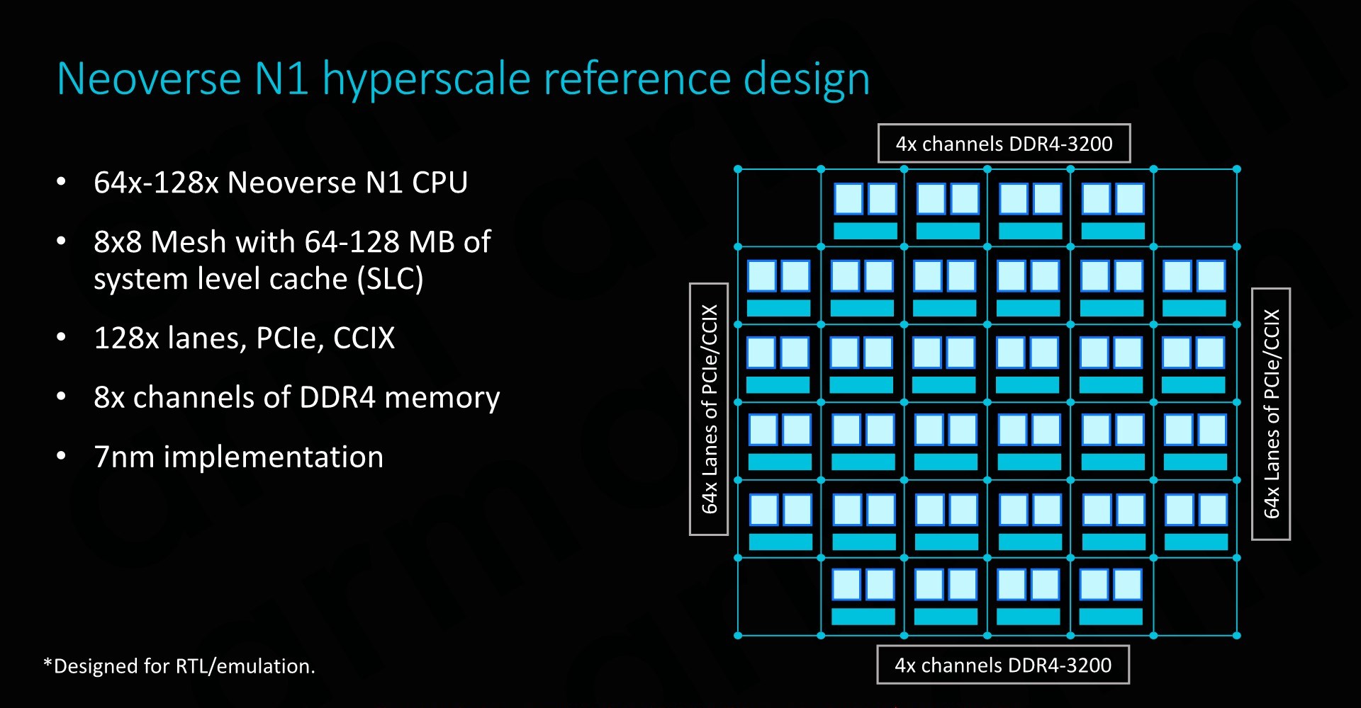
Scaling the design to 128 cores doesn’t represent an issue for the IP, although we’ll be hitting some practical limits in terms of current generation technology. Arm’s 64 core N1 reference design with 64MB of cache on a 7nm process node would result in a die size a little under 400mm², which probably is on the higher end of what vendors would want to target in terms of manufacturability. To alleviate such concerns, Arm also took a page out of AMD’s book and floated the idea of chiplet designs, where each chiplet would communicate over CCIX links. Inherently it’s up to the vendor to decide how they’ll want to design their solution, and Arm provides the essential building blocks and flexibility to enable this.
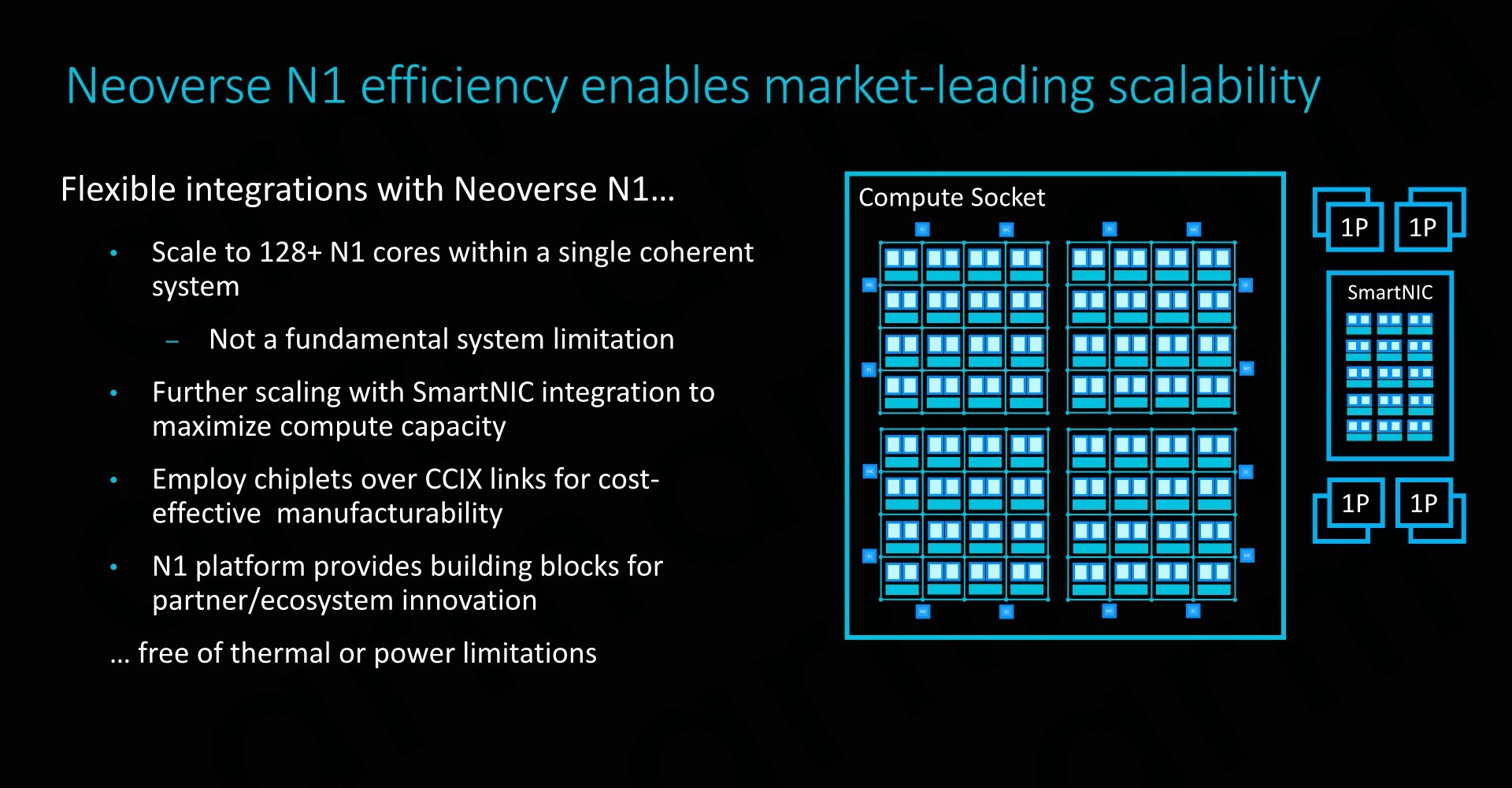
SmartNIC integration capability is also an important aspect of the design and its flexibility. To maximise compute capacity in large scale system, having accelerated network connectivity is key in actually achieving high throughput in the densest (and efficient) form-factor possible.
The CMN-600 allows for slave ports on its crosspoints: Here we can see MMUs connected with high bandwidth interfaces of up to 128GB/s. Attaching fixed-function hardware offloading IP thus would be extremely easy to implement.
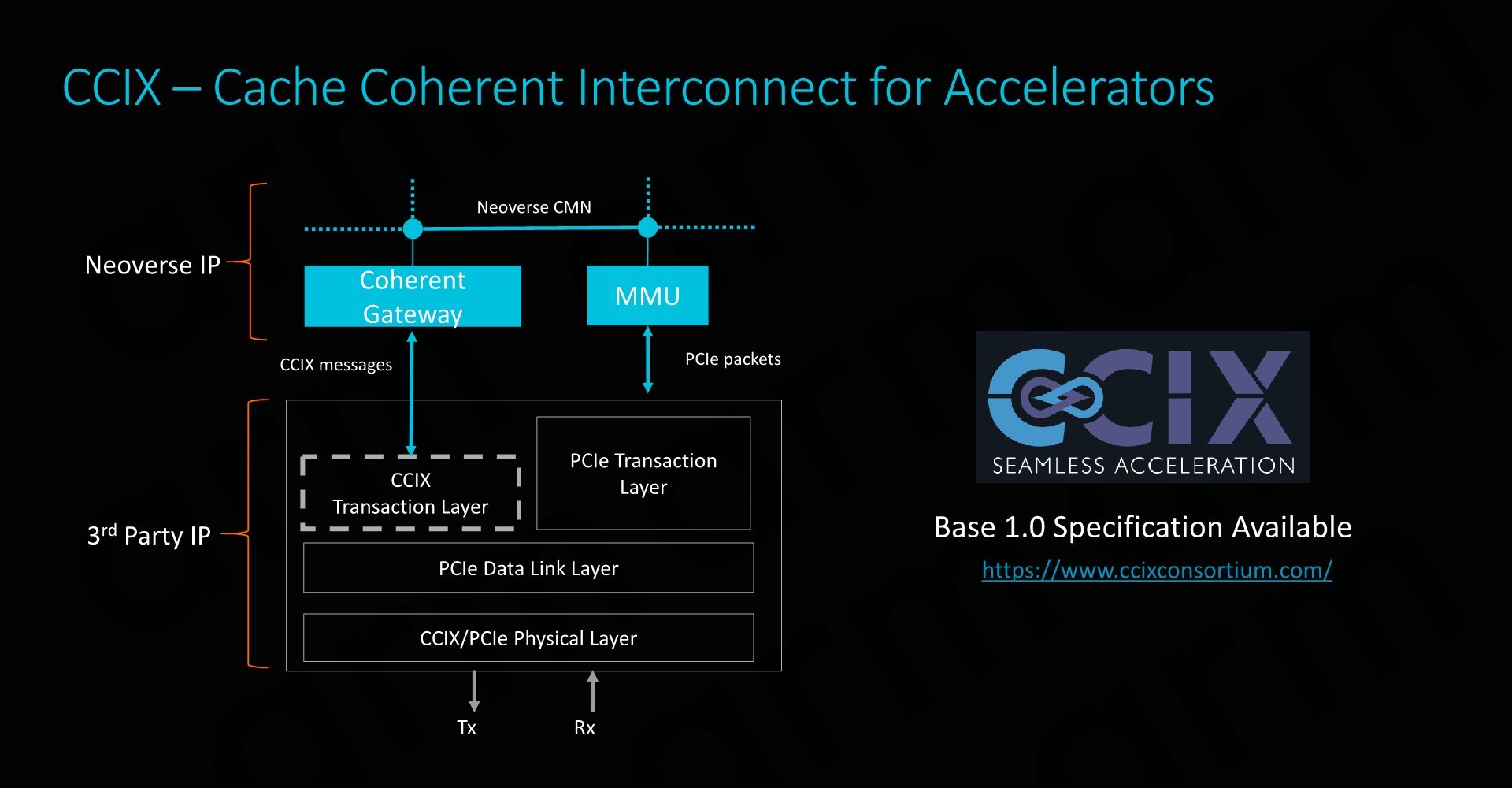
CCIX is extremely important for Arm as it enables its product portfolio to integrate with third-party IP offerings. Enabling cache coherency for external IP blocks is an incredibly attractive feature to have as it massively simplifies software design for the vendors. Essentially what this means is that software simply sees a single huge block of memory, whereas non-coherent systems require drivers and software to be aware and track what part of memory is valid and what isn’t. In terms of IP integration, Arm provides the CCIX coherent gateway that integrates with the CMN-600, while on the other side it’s the onus of the third-party IP provider to provide the CCIX translation layer.
Currently Xilinx will be among the first vendors to offer CCIX-enabled end-products in Q3 2019. With AMD also fully embracing CCIX, there’s some very exciting future potential for third-party accelerator hardware, and we be seeing new use-cases that just weren’t feasible before.
Power/Performance management
While it’s a bit weird to talk about power management in the context of implementation scalability (The average reader might think of it as a thermal/cooling consideration), there’s some very interesting implications in terms of how Arm simplifies the work needed to be done by the vendor.
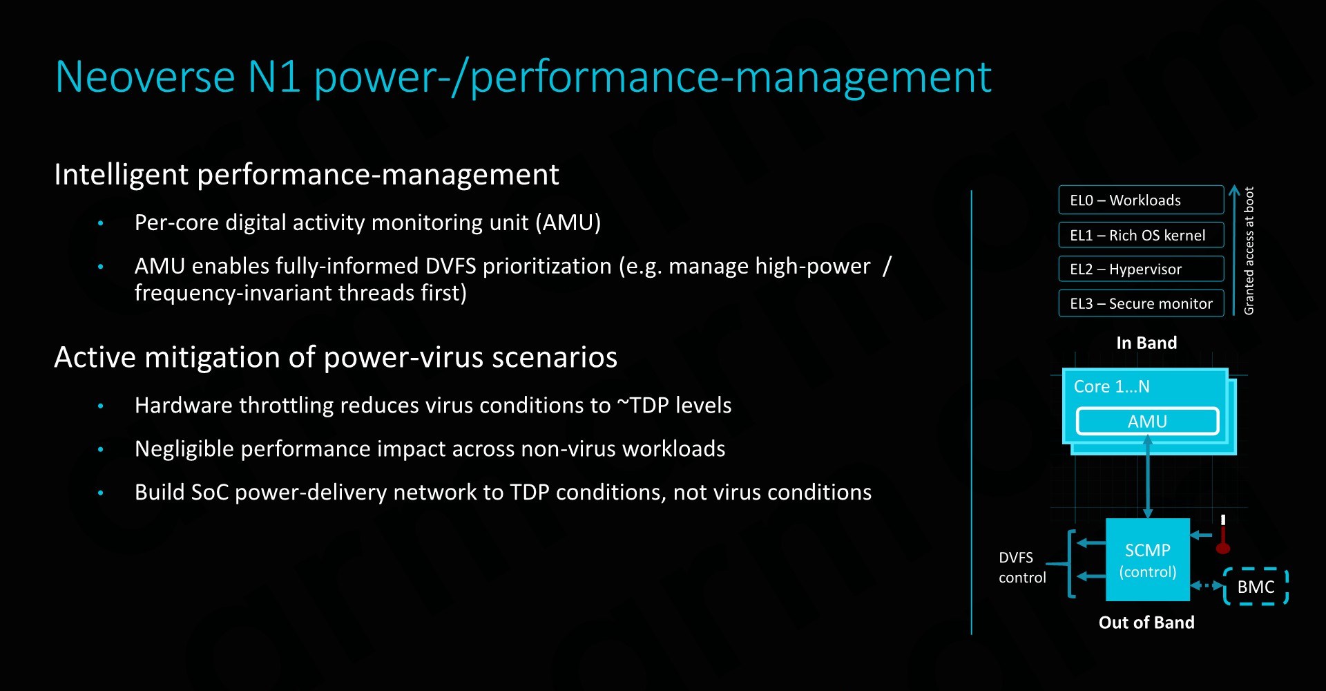
Along a chip’s logical design, a vendor must also implement a power delivery network that will be able to adequately support the IP. In real-world use-cases this means that the PDN needs to be as robust as to deal with the worst-case power scenario of a component. This is actually quite a headache for many vendors as the design requires complex models and in most cases the PDN will need to be over-engineered in order to offer guarantees of stability, which in turn raises the complexity and cost of the implementation.
Arm seeks to alleviate these concerns by offering extremely fine-grained DVFS mechanisms in the form of a dedicated micro-controller. The controller access detailed activity monitoring units inside the CPU cores, seeing what actual blocks and how many transistors are actually actively switching, and feeding this information back to the system controller to change DVFS states. This provides a certain level of hard-guarantee as to when the CPU enters power-virus-like workloads which can cause current spikes, and avoid them in time. This enables vendors to design their PDNs to more conservative tolerances, saving on implementation cost.


101 Comments
View All Comments
blu42 - Thursday, February 21, 2019 - link
Yep. While ISA may not matter as an aggregate over the set of all tasks, ISAs matter very much when it comes to the performance of any individual task, just the same way as ASICs matter versus gen-purpose CPUs for any given task. One can think of ASICs as an extreme-case specialization of gen-purpose ISAs.Meteor2 - Wednesday, February 20, 2019 - link
Indeed, and reality is that all architectures are converging in terms of performance. It’s just a question of how much money any given manufacturer wants to invest. Intel cut R&D and the results are plain. AMD invested wisely. What Apple has achieved with the ARM ISA is phenomenal. Goodness knows what they could do if they turned their attention away from mobile but goodness knows how much it cost, too.Vitor - Wednesday, February 20, 2019 - link
Although the article is about servers and such, I can't help thinking that in less than a decade RISC CPUs can overtake the deskop/notebook market.And, corretct if I'm wrong, RISC is inherently more efficient than X86 derivates.
SarahKerrigan - Wednesday, February 20, 2019 - link
The evidence for "inherently more efficient" is pretty shaky, although I'd venture that validation of ARM cores is considerably simpler than validation of x86.That being said, ARM has been delivering rapidly and consistently on uarch, and Intel has not.
hMunster - Wednesday, February 20, 2019 - link
ARM is playing catch-up to Intel which got to the point of "no more low hanging fruit" much earlier.Wilco1 - Wednesday, February 20, 2019 - link
Well as an example Intel was unable to design competitive SoCs for the mobile market despite having a process advantage, investing $10+ Billion and even paying various companies to use their chips - "contra-revenue". There is no doubt the complexity of x86 translates into a significant overhead in design and verification, area, power and (at the low end) performance.hMunster - Wednesday, February 20, 2019 - link
The RISC vs. CISC debate does not really matter much anymore.HStewart - Wednesday, February 20, 2019 - link
A lot of this is because CISC process can now handle multiple microinstructions per clock cycle taking advantage of RISC smaller instruction away.But software compatibility is the major concern with this and Microsoft has many failed attempts to try to change this dependency.
FunBunny2 - Wednesday, February 20, 2019 - link
"A lot of this is because CISC process can now handle multiple microinstructions per clock cycle taking advantage of RISC smaller instruction away."that's a testable assertion. not by me, however. the execution of multiple microinstructions by CISC ISA machines doesn't mean, ceteris paribus, that the overlying CISC instruction runs as efficiently as a native RISC instruction; it just must run through the microinstructions. to the extent that CISC ISAs are really executed as some RISC machine on the silicon, that doesn't mean, apples to apples, that said CISC machine executes as efficiently as a native RISC machine. (native RISC does make headaches for the compiler writer, no doubt.) I'd wager that the real reason for RISC microarch was the desire to continue with X86 object code with a bit more performance back when the transistor budget began expanding, but not enough to build the entire ISA in silicon. and to keep the compiler writer from having to continually update as the real ISA (RISC) keeps changing. die shots of current cpu show that the 'core' is a diminishing percent of the real estate.
the still unanswered question: why did Intel/AMD not use the exploding transistor budget to execute the entire instruction set in hardware, but to create these behind-the-scenes RISC machines?
wumpus - Wednesday, February 20, 2019 - link
From memory, Dec was able to make VAX four times faster by pipelining the microcode from VAX instructions compared to "executing the VAX instruction all at once faster". VAX was about the CISCisest CISC that ever CISCed (and sold successfully. I think Intel's BiiN was worse).Dec also made Alpha, which even the first iteration was another 4 times faster than the "pipelined microcode" VAX.
And this was all single issue. Don't even think of trying to issue multiple "full CISC" instructions at once.